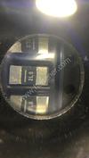
| Part Number | 74LVTH240MTCX |
|---|---|
| Manufacturer | ON Semiconductor |
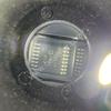
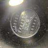
| Description | IC BUFFER INVERT 3.6V 20TSSOP |
| Datasheet | |
| Package | 20-TSSOP (0.173", 4.40mm Width) |
| ECAD |
|
| In Stock | 16,968 piece(s) |
| Unit Price | $ 0.3753 * |
| Lead Time | Can Ship Immediately |
| Estimated Delivery Time | Apr 28 - May 3 (Choose Expedited Shipping) |
| Request for Quotation |
|
| Payment Methods | |
| Delivery Services |
Part Number # 74LVTH240MTCX (Logic - Buffers, Drivers, Receivers, Transceivers) is manufactured by ON Semiconductor and distributed by Heisener. Being one of the leading electronics distributors, we carry many kinds of electronic components from some of the world’s top class manufacturers. Their quality is guaranteed by its stringent quality control to meet all required standards.
For 74LVTH240MTCX specifications/configurations, quotation, lead time, payment terms of further enquiries please have no hesitation to contact us. To process your RFQ, please add 74LVTH240MTCX with quantity into BOM. Heisener.com does NOT require any registration to request a quote of 74LVTH240MTCX.
| Manufacturer | ON Semiconductor |
| Category | Integrated Circuits (ICs) - Logic - Buffers, Drivers, Receivers, Transceivers |
| Package | 20-TSSOP (0.173", 4.40mm Width) |
| ECAD |
|
| Series | 74LVTH |
| Logic Type | Buffer, Inverting |
| Number of Elements | 2 |
| Number of Bits per Element | 4 |
| Input Type | - |
| Output Type | 3-State |
| Current - Output High, Low | 32mA, 64mA |
| Voltage - Supply | 2.7 V ~ 3.6 V |
| Operating Temperature | -40°C ~ 85°C (TA) |
| Mounting Type | Surface Mount |
| Package / Case | 20-TSSOP (0.173", 4.40mm Width) |
| Supplier Device Package | 20-TSSOP |
Miya*****herjee
April 4, 2023
Ray***** Roth
March 31, 2023
Aliy*****sneros
March 30, 2023
Fish*****aylor
March 23, 2023
Russ*****Bhatti
March 10, 2023
Lega*****uang
March 10, 2023
Bexl*****iller
March 3, 2023


|
EMVY630GTR221MLH0S | United Chemi-Con, CAP ALUM 220UF 20% 63V SMD, Radial, Can - SMD, 74LVTH | View |

|
BZX384B4V7-G3-18 | Vishay Semiconductor Diodes Division, DIODE ZENER 4.7V 200MW SOD323, SC-76, SOD-323, 74LVTH | View |

|
M93C66-RDW3TP/K | STMicroelectronics, IC EEPROM 4KBIT 2MHZ 8TSSOP, 8-TSSOP (0.173", 4.40mm Width), 74LVTH | View |

|
SN65MLVD200ADG4 | Texas Instruments, IC M-LVDS LINE DVR/RCVR 8-SOIC, 8-SOIC (0.154", 3.90mm Width), 74LVTH | View |

|
H81K21BDA | TE Connectivity Passive Product, RES 1.21K OHM 1/4W 0.1% AXIAL, Axial, 74LVTH | View |
|
|
ATDB4R | Amphenol PCD, CONN TERM BLK FEED THRU 10-22AWG, -, 74LVTH | View |
|
|
1604290000 | Weidmuller, SLIDE JUMPER WTL/Q/D SAKT 3POS, -, 74LVTH | View |
|
|
FTR-115-54-L-D | Samtec Inc., SMT .050'' STRIPS, -, 74LVTH | View |
|
|
FW-02-01-G-D-200-177 | Samtec Inc., .050'' BOARD SPACERS, -, 74LVTH | View |
|
|
3017W2PAR69F20X | Conec, CONN PLUG MALE PINS 17POS, -, 74LVTH | View |
|
|
M83723/76A24439 | TE Connectivity Deutsch Connectors, CONN PLUG 43POS STRGHT W/PINS, -, 74LVTH | View |

|
VI-J33-IW-S | Vicor Corporation, CONVERTER MOD DC/DC 24V 100W, Half Brick, 74LVTH | View |

We guarantee 100% customer satisfaction.
Our experienced sales team and tech support team back our services to satisfy all our customers.

We provide 90 days warranty.
If the items you received were not in perfect quality, we would be responsible for your refund or replacement, but the items must be returned in their original condition.
| Part Number | Manufacturer | Description | Stock |
74LVTH240MTCX D# V36:1790_06297857 |
ON Semiconductor |
Buffer/Line Driver 8-CH Inverting 3-ST BiCMOS 20-Pin TSSOP T/R RoHS: Compliant
|
0 |
| Part Number | Manufacturer | Description | Stock |
74LVTH240MTCX D# 74LVTH240MTCX |
ON Semiconductor |
Buffer/Line Driver 8-CH Inverting 3-ST BiCMOS 20-Pin TSSOP T/R - Bulk (Alt: 74LVTH240MTCX) |
0 |
| Part Number | Manufacturer | Description | Stock |
74LVTH240MTCX D# 74LVTH240MTCX |
ON Semiconductor |
Buffer/Line Driver 8-CH Inverting 3-ST BiCMOS 20-Pin TSSOP T/R (Alt: 74LVTH240MTCX) |
0 |
| Part Number | Manufacturer | Description | Stock |
74LVTH240MTCX |
Fairchild Semiconductor Corporation | 7500 |
| Part Number | Manufacturer | Description | Stock |
74LVTH240MTCX |
Fairchild Semiconductor Corporation |
IC INVERTER DUAL 4-INPUT 20TSSOP |
0 |
| Part Number | Manufacturer | Description | Stock |
74LVTH240MTCX |
Fairchild Semiconductor Corporation |
2000 |
2500 |
| Part Number | Manufacturer | Description | Stock |
74LVTH240MTCX D# 2156-74LVTH240MTCX-ND |
Rochester Electronics LLC |
IC BUFFER INVERT 3.6V 20TSSOP |
35496 |
| Part Number | Manufacturer | Description | Stock |
74LVTH240MTCX D# 3608911 |
ON Semiconductor |
BUFFERS & TRANSCEIVERS RoHS: Compliant
Min Qty: 2500
Container: Reel
|
0 |
| Part Number | Manufacturer | Description | Stock |
DM74LVTH240MTCX |
Fairchild Semiconductor Corporation |
OEM/CM QUOTES ONLY | NO BROKERS |
325 |
74LVTH240MTCX |
Fairchild Semiconductor Corporation |
OEM/CM QUOTES ONLY | NO BROKERS |
8625 |
| Part Number | Manufacturer | Description | Stock |
74LVTH240MTCXTSSOP20 |
NXP Semiconductors |
OEM/CM ONLY |
2600 |
| Part Number | Manufacturer | Description | Stock |
74LVTH240MTCX D# 512-74LVTH240MTCX |
ON Semiconductor |
Buffers & Line Drivers Octal Buf/Line Drv RoHS: Compliant
|
477 |
| Part Number | Manufacturer | Description | Stock |
74LVTH240MTCX |
Fairchild Semiconductor Corporation | 6000 |
| Part Number | Manufacturer | Description | Stock |
74LVTH240MTCX |
Fairchild Semiconductor Corporation |
Bus Driver, LVT Series, 2-Func, 4-Bit, Inverted Output, BICMOS, PDSO20 RoHS: Compliant
|
35496 |
| Part Number | Manufacturer | Description | Stock |
DM74LVTH240MTCX |
Fairchild Semiconductor Corporation |
OEM/CM ONLY |
294 |
74LVTH240MTCX |
Fairchild Semiconductor Corporation |
OEM/CM ONLY |
25279 |
| Part Number | Manufacturer | Description | Stock |
74LVTH240MTCX D# 26636141 |
ON Semiconductor |
Buffer/Line Driver 8-CH Inverting 3-ST BiCMOS 20-Pin TSSOP T/R RoHS: Compliant
|
0 |
| Part Number | Manufacturer | Description | Stock |
74LVTH240MTCX |
mfr |
RFQ |
11372 |
Heisener's commitment to quality has shaped our processes for sourcing, testing, shipping, and every step in between. This foundation underlies each component we sell.

Do you have any question about 74LVTH240MTCX?
86-755-83210559 x831


Scan to view this page