| Part Number | 74VHC132M |
|---|---|
| Manufacturer | ON Semiconductor |
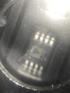
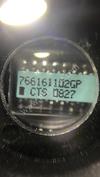
| Description | IC GATE NAND SCHMITT 4CH 14SOIC |
| Datasheet | |
| Package | 14-SOIC (0.154", 3.90mm Width) |
| ECAD |
|
| In Stock | 6,176 piece(s) |
| Unit Price | $ 0.2781 * |
| Lead Time | Can Ship Immediately |
| Estimated Delivery Time | Apr 21 - Apr 26 (Choose Expedited Shipping) |
| Request for Quotation |
|
| Payment Methods | |
| Delivery Services |
Part Number # 74VHC132M (Logic - Gates and Inverters) is manufactured by ON Semiconductor and distributed by Heisener. Being one of the leading electronics distributors, we carry many kinds of electronic components from some of the world’s top class manufacturers. Their quality is guaranteed by its stringent quality control to meet all required standards.
For 74VHC132M specifications/configurations, quotation, lead time, payment terms of further enquiries please have no hesitation to contact us. To process your RFQ, please add 74VHC132M with quantity into BOM. Heisener.com does NOT require any registration to request a quote of 74VHC132M.
| Manufacturer | ON Semiconductor |
| Category | Integrated Circuits (ICs) - Logic - Gates and Inverters |
| Package | 14-SOIC (0.154", 3.90mm Width) |
| ECAD |
|
| Series | 74VHC |
| Logic Type | NAND Gate |
| Number of Circuits | 4 |
| Number of Inputs | 2 |
| Features | Schmitt Trigger |
| Voltage - Supply | 2 V ~ 5.5 V |
| Current - Quiescent (Max) | 2µA |
| Current - Output High, Low | 8mA, 8mA |
| Logic Level - Low | 0.9 V ~ 1.65 V |
| Logic Level - High | 2.2 V ~ 3.85 V |
| Max Propagation Delay @ V, Max CL | 9.7ns @ 5V, 50pF |
| Operating Temperature | -40°C ~ 85°C |
| Mounting Type | Surface Mount |
| Supplier Device Package | 14-SOIC |
| Package / Case | 14-SOIC (0.154", 3.90mm Width) |
Kama*****earson
March 31, 2023
Zayl*****otts
March 29, 2023
Kal*****h Lin
March 28, 2023
Kayla*****tterson
March 18, 2023
Ian*****ntes
March 14, 2023
Dan*****o Wu
March 4, 2023
Aniy*****oone
March 4, 2023
Adela*****avala
February 27, 2023


|
SIT9003AI-2-25DO | SiTIME, OSC PROG LVCMOS 2.5V 50PPM SMD, 4-SMD, No Lead, 74VHC | View |

|
1812J2500561FFR | Knowles Syfer, CAP CER 560PF 250V C0G/NP0 1812, 1812 (4532 Metric), 74VHC | View |

|
C0402C202J4JAC7867 | KEMET, CAP CER 2000PF 16V U2J 0402, 0402 (1005 Metric), 74VHC | View |

|
LXZ35VB102M12X25LL | United Chemi-Con, CAP ALUM 1000UF 20% 35V RADIAL, Radial, Can, 74VHC | View |
|
|
EKMM161VSN122MA30S | United Chemi-Con, CAP ALUM 1200UF 20% 160V SNAP, Radial, Can - Snap-In, 74VHC | View |

|
PUMD6,115 | Nexperia USA Inc., TRANS PREBIAS NPN/PNP 6TSSOP, 6-TSSOP, SC-88, SOT-363, 74VHC | View |

|
PI49FCT807CTSE | Diodes Incorporated, IC CLK BUFFER 1:10 100MHZ 20SOIC, 20-SOIC (0.295", 7.50mm Width), 74VHC | View |
|
|
203-222-2-35211-1 | Sensata Technologies/Airpax, CIR BRKR ROCKER, -, 74VHC | View |

|
1-284046-2 | TE Connectivity AMP Connectors, TERM BLOCK PLUG 12POS 90DEG 5MM, -, 74VHC | View |

|
929705-09-20-I | 3M, CONN HEADER 20POS STR .100" GOLD, -, 74VHC | View |
|
|
FW-10-05-LM-D-355-140-A | Samtec Inc., .050'' BOARD SPACERS, -, 74VHC | View |
|
|
MP8-3E-1L-1L-1A-00 | Artesyn Embedded Technologies, MP CONFIGURABLE POWER SUPPLY, -, 74VHC | View |

We guarantee 100% customer satisfaction.
Our experienced sales team and tech support team back our services to satisfy all our customers.

We provide 90 days warranty.
If the items you received were not in perfect quality, we would be responsible for your refund or replacement, but the items must be returned in their original condition.
| Part Number | Manufacturer | Description | Stock |
74VHC132MTCX D# V36:1790_06298288 |
ON Semiconductor |
NAND Gate 4-Element 2-IN CMOS 14-Pin TSSOP W T/R RoHS: Compliant
|
0 |
74VHC132MX D# P40:2555_16309542 |
ON Semiconductor |
NAND Gate 4-Element 2-IN CMOS 14-Pin SOIC N T/R RoHS: Compliant
|
0 |
74VHC132M D# P40:2555_13152083 |
ON Semiconductor |
NAND Gate 4-Element 2-IN CMOS 14-Pin SOIC N Tube RoHS: Compliant
|
0 |
| Part Number | Manufacturer | Description | Stock |
MC74VHC132M D# MC74VHC132M |
NXP Semiconductors |
- Bulk (Alt: MC74VHC132M) RoHS: Not Compliant
|
0 |
74VHC132M D# 74VHC132M |
ON Semiconductor |
NAND Gate 4-Element 2-IN CMOS 14-Pin SOIC N Rail - Bulk (Alt: 74VHC132M) |
0 |
74VHC132MTCX D# 74VHC132MTCX |
ON Semiconductor |
NAND Gate 4-Element 2-IN CMOS 14-Pin TSSOP T/R - Bulk (Alt: 74VHC132MTCX) |
0 |
MC74VHC132MELG D# MC74VHC132MELG |
ON Semiconductor |
NAND Gate 4-Element 2-IN CMOS 14-Pin SO EIAJ T/R - Bulk (Alt: MC74VHC132MELG) |
0 |
MC74VHC132MEL D# MC74VHC132MEL |
ON Semiconductor |
- Bulk (Alt: MC74VHC132MEL) |
0 |
74VHC132MX D# 74VHC132MX |
ON Semiconductor |
NAND Gate 4-Element 2-IN CMOS 14-Pin SOIC N T/R - Bulk (Alt: 74VHC132MX) RoHS: Compliant
|
0 |
74VHC132MTC D# 74VHC132MTC |
ON Semiconductor |
- Bulk (Alt: 74VHC132MTC) RoHS: Compliant
|
0 |
| Part Number | Manufacturer | Description | Stock |
74VHC132MX D# 74VHC132MX |
ON Semiconductor |
NAND Gate 4-Element 2-IN CMOS 14-Pin SOIC N T/R (Alt: 74VHC132MX) RoHS: Compliant
|
0 |
| Part Number | Manufacturer | Description | Stock |
74VHC132MTCX D# 74VHC132MTCX |
ON Semiconductor |
NAND Gate 4-Element 2-IN CMOS 14-Pin TSSOP T/R (Alt: 74VHC132MTCX) |
0 |
74VHC132MX D# 74VHC132MX |
ON Semiconductor |
NAND Gate 4-Element 2-IN CMOS 14-Pin SOIC N T/R (Alt: 74VHC132MX) |
0 |
74VHC132M D# 74VHC132M |
ON Semiconductor |
NAND Gate 4-Element 2-IN CMOS 14-Pin SOIC N Rail (Alt: 74VHC132M) |
0 |
| Part Number | Manufacturer | Description | Stock |
74VHC132MX |
Fairchild Semiconductor Corporation | 19280 | |
74VHC132MTCX |
Fairchild Semiconductor Corporation | 737 |
| Part Number | Manufacturer | Description | Stock |
74VHC132MTC |
Fairchild Semiconductor Corporation |
- Tape and Reel |
32500 |
74VHC132M |
Fairchild Semiconductor Corporation |
- Tape and Reel |
32500 |
74VHC132MX |
Fairchild Semiconductor Corporation |
IC GATE NAND 4CH 2-INP 14-SO |
2500 |
74VHC132MTCX |
Fairchild Semiconductor Corporation |
- Tape and Reel |
32500 |
MC74VHC132MELG |
ON Semiconductor |
N/A AHC/VHC SERIES, QUAD 2-INPUT NAND GATE, PDSO14 LEAD FREE, EIAJ, SO-14 |
31978 |
| Part Number | Manufacturer | Description | Stock |
74VHC132M |
Fairchild Semiconductor Corporation |
NAND Gate, AHC/VHC Series, 4-Func, 2-Input, CMOS, PDSO14 RoHS: Compliant
|
0 |
74VHC132MTCX |
Fairchild Semiconductor Corporation |
NAND Gate, AHC/VHC Series, 4-Func, 2-Input, CMOS, PDSO14 RoHS: Not Compliant
|
0 |
| Part Number | Manufacturer | Description | Stock |
74VHC132M D# 74VHC132MFS-ND |
ON Semiconductor |
IC GATE NAND 4CH 2-INP 14SOIC |
1186 |
74VHC132MTC D# 2156-74VHC132MTC-FS-ND |
Rochester Electronics LLC |
IC GATE NAND 4CH 2-INP 14TSSOP |
45190 |
74VHC132MX D# 74VHC132MXCT-ND |
ON Semiconductor |
IC GATE NAND 4CH 2-INP 14SOIC |
1196 |
MC74VHC132M D# 2156-MC74VHC132M-ND |
Rochester Electronics LLC |
NAND GATE, AHC/VHC SERIES, 4-FUN |
450 |
MC74VHC132MELG D# 2156-MC74VHC132MELG-ND |
Rochester Electronics LLC |
IC GATE NAND 4CH 2-INP SOEIAJ |
31978 |
MC74VHC132MEL D# 2156-MC74VHC132MEL-ND |
Rochester Electronics LLC |
NAND GATE, AHC/VHC SERIES |
1097 |
74VHC132MTCX D# 74VHC132MTCXCT-ND |
ON Semiconductor |
IC GATE NAND 4CH 2-INP 14TSSOP |
2337 |
| Part Number | Manufacturer | Description | Stock |
74VHC132MX |
Fairchild Semiconductor Corporation |
In stock shipping within 2days |
788 |
MC74VHC132MEL |
Motorola Semiconductor Products |
In stock shipping within 2days |
3760 |
74VHC132MTCX |
Fairchild Semiconductor Corporation |
In stock shipping within 2days |
6760 |
| Part Number | Manufacturer | Description | Stock |
74VHC132M D# 1014114 |
ON Semiconductor |
74VHC CMOS, SMD, 74VHC132, SOIC14 RoHS: Compliant
Min Qty: 1
Container: Each
|
581 |
74VHC132MTCX D# 2453079RL |
ON Semiconductor |
NAND GATE, SCHMITT, QUAD, 2 I/P, TSSOP14 RoHS: Compliant
Min Qty: 5
Container: Reel
|
0 |
74VHC132MX D# 3609684 |
ON Semiconductor |
NAND GATE, 2 I/P, -40 TO 85DEG C RoHS: Compliant
Min Qty: 2500
Container: Reel
|
0 |
| Part Number | Manufacturer | Description | Stock |
74VHC132MX |
ON Semiconductor |
74VHC Series High Speed CMOS Quad 2-Input NAND Schmitt Trigger - SOIC-14 RoHS: Compliant
pbFree: Yes
|
2500 |
74VHC132MTCX |
ON Semiconductor |
74VHC Series High Speed CMOS Quad 2-Input NAND Schmitt Trigger - TSSOP-14 RoHS: Compliant
pbFree: Yes
|
2500 |
74VHC132M |
ON Semiconductor |
74VHC Series Quad 2-Input NAND Surface Mount Schmitt Trigger - SOIC-14 RoHS: Compliant
pbFree: Yes
|
0 |
| Part Number | Manufacturer | Description | Stock |
MC74VHC132MEL |
ON SEMICONDUCTOR |
OEM/CM QUOTES ONLY | NO BROKERS |
2029 |
74VHC132MTC |
Rochester Electronics LLC |
OEM/CM QUOTES ONLY | NO BROKERS |
51969 |
274VHC132MTCX |
ON Semiconductor |
OEM/CM QUOTES ONLY | NO BROKERS |
39383 |
74VHC132M |
Fairchild Semiconductor Corporation |
OEM/CM QUOTES ONLY | NO BROKERS |
6452 |
74VHC132MTR |
STMicroelectronics |
OEM/CM QUOTES ONLY | NO BROKERS |
14375 |
74VHC132MTCXNL |
w/a |
OEM/CM QUOTES ONLY | NO BROKERS |
1403 |
MC74VHC132MELG |
Rochester Electronics LLC |
OEM/CM QUOTES ONLY | NO BROKERS |
37094 |
74VHC132MTCX |
ON SEMICONDUCTOR |
OEM/CM QUOTES ONLY | NO BROKERS |
83375 |
74VHC132MX |
ON Semiconductor |
OEM/CM QUOTES ONLY | NO BROKERS |
20125 |
| Part Number | Manufacturer | Description | Stock |
74VHC132MTCX |
Texas Instruments |
in stock - can ship the same day |
130 |
74VHC132M |
Amphenol FCi |
in stock - can ship the same day |
47 |
| Part Number | Manufacturer | Description | Stock |
74VHC132MX |
National Semiconductor Corporation |
OEM/CM Immediate delivery |
5000 |
74VHC132MTCX |
Fairchild Semiconductor Corporation |
OEM/CM Immediate delivery |
68900 |
MC74VHC132MEL |
Motorola Semiconductor Products |
OEM/CM Immediate delivery |
3500 |
| Part Number | Manufacturer | Description | Stock |
74VHC132MTCX D# 512-74VHC132MTCX |
ON Semiconductor |
Logic Gates Qd 2-In NAND Sc Trig RoHS: Compliant
|
3123 |
74VHC132MX D# 512-74VHC132MX |
ON Semiconductor |
Logic Gates Qd 2-In NAND Sc Trig RoHS: Compliant
|
5304 |
74VHC132M D# 512-74VHC132M |
ON Semiconductor |
Logic Gates Qd 2-In NAND Sc Trig RoHS: Compliant
|
4041 |
| Part Number | Manufacturer | Description | Stock |
74VHC132MX D# XSFP00000173116 |
Fairchild Semiconductor Corporation |
74VHC Series High Speed CMOS Quad 2-Input NAND Schmitt Trigger - SOIC-14 |
5000 |
74VHC132MTCX D# XSFP00000001920 |
Fairchild Semiconductor Corporation |
74VHC Series High Speed CMOS Quad 2-Input NAND Schmitt Trigger - TSSOP-14 |
10000 |
| Part Number | Manufacturer | Description | Stock |
74VHC132M D# 26AC8734 |
ON Semiconductor |
QUAD 2-INPUT NAND SCHMITT ROHS COMPLIANT: YES RoHS: Compliant
Min Qty: 3300
Container: Bulk
|
0 |
74VHC132MTCX D# 84AC3973 |
ON Semiconductor |
QUAD 2-INPUT NAND SCHMITT ROHS COMPLIANT: YES RoHS: Compliant
Min Qty: 2500
Container: TAPE & REEL - FULL
|
0 |
74VHC132MX. D# 61AC3917 |
ON Semiconductor |
Logic Function:NAND Gate, No. of Elements:Quad, No. of Inputs:2Inputs, No. of Pins:14Pins, Logic Case Style:SOIC, Product Range:74VHC132, Logic IC Family:74VHC, Supply Voltage Min:2V, Supply Voltage Max:5.5V, Output Current:8mA RoHS Compliant: Yes RoHS: Compliant
Min Qty: 5000
Container: TAPE & REEL - FULL
|
0 |
| Part Number | Manufacturer | Description | Stock |
74VHC132MTCX D# NS-74VHC132MTCX |
Fairchild Semiconductor Corporation |
OEM/CM ONLY |
6481 |
74VHC132M D# NS-74VHC132M |
Fairchild Semiconductor Corporation |
OEM/CM ONLY |
3987 |
MC74VHC132M D# NS-MC74VHC132M |
VARIOUS |
OEM/CM ONLY |
1662 |
74VHC132MX D# NS-74VHC132MX |
Fairchild Semiconductor Corporation |
OEM/CM ONLY |
2687 |
74VHC132MTCX(LF) D# NS-74VHC132MTCX(LF) |
Fairchild Semiconductor Corporation |
OEM/CM ONLY |
9630 |
MC74VHC132ML1 D# NS-MC74VHC132ML1 |
ON Semiconductor |
OEM/CM ONLY |
1543 |
MC74VHC132MEL D# NS-MC74VHC132MEL |
ON Semiconductor |
OEM/CM ONLY |
3864 |
MC74VHC132MELG D# NS-MC74VHC132MELG |
ON Semiconductor |
OEM/CM ONLY |
7763 |
MC74VHC132ML2 D# NS-MC74VHC132ML2 |
ON Semiconductor |
OEM/CM ONLY |
2264 |
| Part Number | Manufacturer | Description | Stock |
74VHC132MTCX |
Fairchild Semiconductor Corporation |
AHC/VHC SERIES, QUAD 2-INPUT NAND GATE, PDSO14 |
188 |
74VHC132M |
Fairchild Semiconductor Corporation |
AHC/VHC SERIES, QUAD 2-INPUT NAND GATE, PDSO14 |
740 |
74VHC132MX |
Fairchild Semiconductor Corporation |
NAND GATE, AHC/VHC SERIES, 4-FUNC, 2-INPUT, CMOS, PDSO14 |
2340 |
| Part Number | Manufacturer | Description | Stock |
74VHC132MTCX D# 74VHC132MTCX |
National Semiconductor Corporation |
Semiconductor |
1605 |
| Part Number | Manufacturer | Description | Stock |
74VHC132M D# 8067109 |
ON Semiconductor |
ON Semiconductor 74VHC132M, Quad 2-Input NAND Schmitt Trigger Logic Gate, 14-Pin SOIC, TU Min Qty: 55
Container: Tube
|
1210 |
| Part Number | Manufacturer | Description | Stock |
74VHC132MTC |
Fairchild Semiconductor Corporation |
NAND Gate, AHC/VHC Series, 4-Func, 2-Input, CMOS, PDSO14 RoHS: Compliant
|
45190 |
74VHC132MX |
ON Semiconductor |
NAND Gate, AHC/VHC Series, 4-Func, 2-Input, CMOS, PDSO14 RoHS: Compliant
|
2500 |
MC74VHC132M |
Motorola Mobility LLC |
NAND Gate, AHC/VHC Series, 4-Func, 2-Input PDSO14 RoHS: Not Compliant
|
450 |
MC74VHC132MELG |
ON Semiconductor |
NAND Gate, AHC/VHC Series, 4-Func, 2-Input, CMOS, PDSO14 RoHS: Compliant
|
31978 |
MC74VHC132MEL |
ON Semiconductor |
NAND Gate, AHC/VHC Series, 4-Func, 2-Input, CMOS, PDSO14 RoHS: Compliant
|
1097 |
74VHC132MTCX |
Fairchild Semiconductor Corporation |
NAND Gate, AHC/VHC Series, 4-Func, 2-Input, CMOS, PDSO14 RoHS: Compliant
|
71196 |
74VHC132M |
ON Semiconductor |
NAND Gate, AHC/VHC Series, 4-Func, 2-Input, CMOS, PDSO14 RoHS: Compliant
|
22715 |
| Part Number | Manufacturer | Description | Stock |
74VHC132MX |
Fairchild Semiconductor Corporation |
OEM/CM ONLY |
40259 |
74VHC132MTC |
Fairchild Semiconductor Corporation |
OEM/CM ONLY |
3440 |
74VHC132MTCX |
Fairchild Semiconductor Corporation |
OEM/CM ONLY |
69660 |
274VHC132MTCX |
ON Semiconductor |
OEM/CM ONLY |
25653 |
74VHC132M |
Fairchild Semiconductor Corporation |
OEM/CM ONLY |
5740 |
74VHC132MTR |
STMicroelectronics |
OEM/CM ONLY |
20902 |
74VHC132MTCXNL |
Fairchild Semiconductor Corporation |
OEM/CM ONLY |
1236 |
| Part Number | Manufacturer | Description | Stock |
MC74VHC132MEL |
Motorola Semiconductor Products |
IN stock Immediate delivery |
3515 |
74VHC132MTCX |
Fairchild Semiconductor Corporation |
IN stock Immediate delivery |
68885 |
74VHC132MX |
National Semiconductor Corporation |
IN stock Immediate delivery |
5015 |
| Part Number | Manufacturer | Description | Stock |
MC74VHC132MEL |
Motorola Mobility LLC |
shipping today |
451 |
74VHC132MTCX |
RF Solutions LTD |
shipping today |
4996 |
74VHC132MX |
Fairchild Semiconductor Corporation |
shipping today |
2866 |
| Part Number | Manufacturer | Description | Stock |
74VHC132M D# 26636260 |
ON Semiconductor |
NAND Gate 4-Element 2-IN CMOS 14-Pin SOIC N Tube RoHS: Compliant
|
0 |
74VHC132MTCX D# 36831593 |
ON Semiconductor |
NAND Gate 4-Element 2-IN CMOS 14-Pin TSSOP W T/R RoHS: Compliant
|
0 |
| Part Number | Manufacturer | Description | Stock |
74VHC132MX |
mfr |
RFQ |
5615 |
| Part Number | Manufacturer | Description | Stock |
74VHC132MTCX D# 2453079RL |
ON Semiconductor |
NAND GATE, SCHMITT, QUAD, 2 I/P, TSSOP14 RoHS: Compliant
Min Qty: 1
Container: Reel
|
0 |
74VHC132MTCX.. D# 1302646 |
ON Semiconductor |
RoHS: Compliant
Min Qty: 1
Container: Cut Tape
|
0 |
74VHC132M D# 1014114 |
ON Semiconductor |
74VHC CMOS, SMD, 74VHC132, SOIC14 RoHS: Compliant
Min Qty: 1
Container: Each
|
131 |
Heisener's commitment to quality has shaped our processes for sourcing, testing, shipping, and every step in between. This foundation underlies each component we sell.

Do you have any question about 74VHC132M?
+86-755-83210559 ext. 805


Scan to view this page