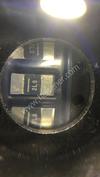
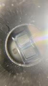
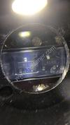
| Part Number | AD5313BRUZ |
|---|---|
| Manufacturer | Analog Devices Inc. |
| Description | IC DAC 10BIT SRL 16TSSOP |
| Datasheet | |
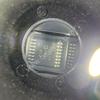
| Package | 16-TSSOP (0.173", 4.40mm Width) |
| ECAD |
|
| In Stock | 95,436 piece(s) |
| Unit Price | $ 11.2243 * |
| Lead Time | Can Ship Immediately |
| Estimated Delivery Time | Apr 28 - May 3 (Choose Expedited Shipping) |
| Request for Quotation |
|
| Payment Methods | |
| Delivery Services |
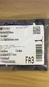
Part Number # AD5313BRUZ (Data Acquisition - Digital to Analog Converters (DAC)) is manufactured by Analog Devices Inc. and distributed by Heisener. Being one of the leading electronics distributors, we carry many kinds of electronic components from some of the world’s top class manufacturers. Their quality is guaranteed by its stringent quality control to meet all required standards.
For AD5313BRUZ specifications/configurations, quotation, lead time, payment terms of further enquiries please have no hesitation to contact us. To process your RFQ, please add AD5313BRUZ with quantity into BOM. Heisener.com does NOT require any registration to request a quote of AD5313BRUZ.
| Manufacturer | Analog Devices Inc. |
| Category | Integrated Circuits (ICs) - Data Acquisition - Digital to Analog Converters (DAC) |
| Package | 16-TSSOP (0.173", 4.40mm Width) |
| ECAD |
|
| Series | - |
| Number of Bits | 10 |
| Number of D/A Converters | 2 |
| Settling Time | 9µs |
| Output Type | Voltage - Buffered |
| Differential Output | No |
| Data Interface | SPI, DSP |
| Reference Type | External |
| Voltage - Supply, Analog | 2.5 V ~ 5.5 V |
| Voltage - Supply, Digital | 2.5 V ~ 5.5 V |
| INL/DNL (LSB) | ±0.5, ±0.05 |
| Architecture | String DAC |
| Operating Temperature | -40°C ~ 105°C |
| Package / Case | 16-TSSOP (0.173", 4.40mm Width) |
| Supplier Device Package | 16-TSSOP |
| Mounting Type | - |
Alai*****hields
April 9, 2023
Brayso*****henson
March 17, 2023
Ayla*****dges
March 14, 2023
Quin*****ibson
March 13, 2023
Tenle*****hanan
March 1, 2023
Kyr*****hana
February 28, 2023


|
ABM10AIG-27.000MHZ-4Z-T3 | Abracon LLC, CRYSTAL 27MHZ 10PF SMD, 4-SMD, No Lead, - | View |

|
1808J0250151FCR | Knowles Syfer, CAP CER 150PF 25V C0G/NP0 1808, 1808 (4520 Metric), - | View |
|
|
B43630A2338M000 | EPCOS (TDK), CAP ALUM 3300UF 20% 200V SNAP, Radial, Can - Snap-In, - | View |
|
|
MRF5S19090HSR3 | NXP, FET RF 65V 1.99GHZ NI-780S, NI-780S, - | View |
 
|
MPC17531ATEP | NXP, IC MOTOR DRIVER PAR 24QFN, 24-VFQFN Exposed Pad, - | View |

|
8N3Q001LG-1053CDI | IDT, Integrated Device Technology Inc, IC OSC CLOCK QD FREQ 10CLCC, 10-CLCC, - | View |

|
SFR2500002409FR500 | Vishay BC Components, RES 24 OHM 0.4W 1% AXIAL, Axial, - | View |

|
HRG3216P-1152-B-T1 | Susumu, RES SMD 11.5K OHM 0.1% 1W 1206, 1206 (3216 Metric), - | View |
|
|
20SRB1-X | TE Connectivity Corcom Filters, PWR ENT RCPT IEC320-C20 PANEL QC, -, - | View |
|
|
10-107618-22P | Amphenol Industrial Operations, CONN PLUG 3POS INLINE PIN, -, - | View |
|
|
EMC44DRTF | Sullins Connector Solutions, CONN EDGE DUAL FMALE 88POS 0.100, -, - | View |
|
|
RMC20DRYN | Sullins Connector Solutions, CONN EDGE DUAL FMALE 40POS 0.100, -, - | View |

We guarantee 100% customer satisfaction.
Our experienced sales team and tech support team back our services to satisfy all our customers.

We provide 90 days warranty.
If the items you received were not in perfect quality, we would be responsible for your refund or replacement, but the items must be returned in their original condition.
| Part Number | Manufacturer | Description | Stock |
AD5313BRUZ D# V99:2348_06207696 |
Analog Devices Inc |
DAC 2-CH Resistor-String 10-bit 16-Pin TSSOP Tube RoHS: Compliant
|
0 |
AD5313BRUZ-REEL7 D# V36:1790_06207700 |
Analog Devices Inc |
DAC 2-CH Resistor-String 10-bit 16-Pin TSSOP T/R RoHS: Compliant
|
0 |
| Part Number | Manufacturer | Description | Stock |
AD5313BRUZ-REEL |
Analog Devices Inc |
CONVERTER - DAC |
0 |
AD5313BRUZ |
Analog Devices Inc |
CONVERTER - DAC |
0 |
AD5313BRUZ-REEL7 |
Analog Devices Inc |
CONVERTER - DAC |
0 |
| Part Number | Manufacturer | Description | Stock |
AD5313BRUZ-REEL7 D# AD5313BRUZ-REEL7TR-ND |
Analog Devices Inc |
IC DAC 10BIT V-OUT 16TSSOP |
0 |
AD5313BRUZ D# AD5313BRUZ-ND |
Analog Devices Inc |
IC DAC 10BIT V-OUT 16TSSOP |
578 |
AD5313BRUZ-REEL D# AD5313BRUZ-REEL-ND |
Analog Devices Inc |
IC DAC 10BIT V-OUT 16TSSOP |
0 |
| Part Number | Manufacturer | Description | Stock |
AD5313BRUZ-REEL |
Analog Devices Inc |
In stock shipping within 2days |
1000 |
AD5313BRUZ |
Analog Devices Inc |
In stock shipping within 2days |
1000 |
| Part Number | Manufacturer | Description | Stock |
AD5313BRUZ D# 2461362 |
Analog Devices Inc |
DAC, DUAL, 10BIT, 143KSPS, TSSOP-16 RoHS: Compliant
Min Qty: 1
Container: Each
|
0 |
| Part Number | Manufacturer | Description | Stock |
AD5313BRUZ |
Analog Devices Inc |
OEM/CM QUOTES ONLY | NO BROKERS |
2092 |
| Part Number | Manufacturer | Description | Stock |
AD5313BRUZREEL7 |
Analog Devices Inc |
OEM/CM ONLY |
272 |
AD5313BRUZ |
Analog Devices Inc |
OEM/CM ONLY |
290 |
AD5313BRUZREEL |
Analog Devices Inc |
OEM/CM ONLY |
271 |
AD5313BRUZ1 |
Analog Devices Inc |
OEM/CM ONLY |
270 |
| Part Number | Manufacturer | Description | Stock |
AD5313BRUZ D# 584-AD5313BRUZ |
Analog Devices Inc |
Digital to Analog Converters - DAC DUAL 10-BIT VOLTAGE OUT DAC I.C. RoHS: Compliant
|
46 |
| Part Number | Manufacturer | Description | Stock |
AD5313BRUZ D# NS-AD5313BRUZ |
Multiple |
OEM/CM ONLY |
2708 |
AD5313BRUZ-REEL D# NS-AD5313BRUZ-REEL |
Analog Devices Inc |
OEM/CM ONLY |
5396 |
AD5313BRUZ-REEL7 D# NS-AD5313BRUZ-REEL7 |
Analog Devices Inc |
OEM/CM ONLY |
5341 |
| Part Number | Manufacturer | Description | Stock |
AD5313BRUZ D# AD5313BRUZ |
Analog Devices Inc |
CONVERTER - DAC RoHS: Compliant
|
0 |
AD5313BRUZ-REEL7 D# AD5313BRUZ-R7 |
Analog Devices Inc |
CONVERTER - DAC RoHS: Compliant
|
0 |
| Part Number | Manufacturer | Description | Stock |
AD5313BRUZ |
Analog Devices Inc |
AD5313 - Dual, 10-Bit nanoDAC with Reference, SPI Interface RoHS: Compliant
|
25 |
| Part Number | Manufacturer | Description | Stock |
AD5313BRUZ |
Analog Devices Inc |
OEM/CM ONLY |
301 |
| Part Number | Manufacturer | Description | Stock |
AD5313BRUZ-REEL |
Analog Devices Inc |
shipping today |
989 |
AD5313BRUZ |
Analog Devices Inc |
shipping today |
2546 |
| Part Number | Manufacturer | Description | Stock |
AD5313BRUZ D# 26615707 |
Analog Devices Inc |
DAC 2-CH Resistor-String 10-bit 16-Pin TSSOP Tube RoHS: Compliant
|
0 |
| Part Number | Manufacturer | Description | Stock |
AD5313BRUZ |
Analog Devices Inc |
RFQ |
2134 |
| Part Number | Manufacturer | Description | Stock |
AD5313BRUZ D# 2461362 |
Analog Devices Inc |
DAC, DUAL, 10BIT, 143KSPS, TSSOP-16 RoHS: Compliant
Min Qty: 1
Container: Each
|
0 |
Heisener's commitment to quality has shaped our processes for sourcing, testing, shipping, and every step in between. This foundation underlies each component we sell.

Do you have any question about AD5313BRUZ?
86-755-83210559 x831


Scan to view this page