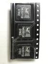
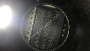
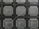
Part Number | C8051F126-GQR |
---|---|
Manufacturer | Silicon Labs |
Description | IC MCU 8BIT 128KB FLASH 100TQFP |
Datasheet | C8051F126-GQR Datasheet |
Package | 100-TQFP |
In Stock | 12,918 piece(s) |
Unit Price | $ 13.9894 * |
Lead Time | Can Ship Immediately |
Estimated Delivery Time | Jan 21 - Jan 26 (Choose Expedited Shipping) |
Request for Quotation |
|
Part Number # C8051F126-GQR (Embedded - Microcontrollers) is manufactured by Silicon Labs and distributed by Heisener. Being one of the leading electronics distributors, we carry many kinds of electronic components from some of the world’s top class manufacturers. Their quality is guaranteed by its stringent quality control to meet all required standards.
For C8051F126-GQR specifications/configurations, quotation, lead time, payment terms of further enquiries please have no hesitation to contact us. To process your RFQ, please add C8051F126-GQR with quantity into BOM. Heisener.com does NOT require any registration to request a quote of C8051F126-GQR.
Manufacturer | Silicon Labs |
Category | Integrated Circuits (ICs) - Embedded - Microcontrollers |
Datasheet | C8051F126-GQRDatasheet |
Package | 100-TQFP |
Series | C8051F12x |
Core Processor | 8051 |
Core Size | 8-Bit |
Speed | 50MHz |
Connectivity | EBI/EMI, SMBus (2-Wire/I2C), SPI, UART/USART |
Peripherals | Brown-out Detect/Reset, POR, PWM, Temp Sensor, WDT |
Number of I/O | 64 |
Program Memory Size | 128KB (128K x 8) |
Program Memory Type | FLASH |
EEPROM Size | - |
RAM Size | 8.25K x 8 |
Voltage - Supply (Vcc/Vdd) | 2.7 V ~ 3.6 V |
Data Converters | A/D 8x8b, 8x10b; D/A 2x12b |
Oscillator Type | Internal |
Operating Temperature | -40°C ~ 85°C (TA) |
Mounting Type | - |
Package / Case | 100-TQFP |
Supplier Device Package | 100-TQFP (14x14) |
8K ISP FLASH MCU Family C8051F120/1/2/3/4/5/6/7 ReAnalog Peripherals - 10 or 12-bit SAR ADC • ± 1 LSB INL • Programmable throughput up to 100 ksps • Up to 8 external inputs; programmable as single- ended or differential • Programmable amplifier gain: 16, 8, 4, 2, 1, 0.5 • Data-dependent windowed interrupt generator • Built-in temperature sensor - 8-bit SAR ADC (‘F12x Only) • Programmable throughput up to 500 ksps • 8 external inputs (single-ended or differential) • Programmable amplifier gain: 4, 2, 1, 0.5 - Two 12-bit DACs (‘F12x Only) • Can synchronize outputs to timers for jitter-free wave- form generation - Two Analog Comparators - Voltage Reference - VDD Monitor/Brown-Out Detector On-Chip JTAG Debug & Boundary Scan - On-chip debug circuitry facilitates full-speed, non- intrusive in-circuit/in-system debugging - Provides breakpoints, single-stepping, watchpoints, stack monitor; inspect/modify memory and registers - Superior performance to emulation systems using ICE-chips, target pods, and sockets - IEEE1149.1 compliant boundary scan - Complete development kit 100-Pin TQFP or 64-Pin TQFP Packaging - Temperature Range: –40 to +85 °C - RoHS Available High Speed 8051 µC Core - Pipelined instruction architecture; executes 70% of instruction set in 1 or 2 system clocks - 100 MIPS or 50 MIPS throughput with on-chip PLL - 2-cycle 16 x 16 MAC engine (C8051F120/1/2/3 and C8051F130/1/2/3 only) Memory - 8448 bytes internal data RAM (8 k + 256) - 128 or 64 kB Banked Flash; in-system programma- ble in 1024-byte sectors - External 64 kB data memory interface (programma- ble multiplexed or non-multiplexed modes) Digital Peripherals - 8 byte-wide port I/O (100TQFP); 5 V tolerant - 4 Byte-wide port I/O (64TQFP); 5 V tolerant - Hardware SMBus™ (I2C™ Compatible), SPI™, and two UART serial ports available concurrently - Programmable 16-bit counter/timer array with 6 capture/compare modules - 5 general purpose 16-bit counter/timers - Dedicated watchdog timer; bi-directional reset pin Clock Sources - Internal precision oscillator: 24.5 MHz - Flexible PLL technology - External Oscillator: Crystal, RC, C, or clock Voltage Supples - Range: 2.7–3.6 V (50 MIPS) 3.0–3.6 V (100 MIPS) - Power saving sleep and shutdown modesv. 1.4 12/03 Copyright © 2003 by Silicon Laboratories C8051F120/1/2/3/4/5/6/7 C8051F130/1/2/3 JTAG 128/64 kB ISP FLASH 8448 B SRAM 16 x 16 MAC ('F120/1/2/3, 'F13x) + - 10/12-bit 100ksps ADC CLOCK / PLL CIRCUIT PGA VREF 12-Bit DAC TEMP SENSOR VOLTAGE COMPARATORS ANALOG PERIPHERALS Port 0 Port 1 Port 2 Port 3 C R O S S B A R DIGITAL I/O HIGH-SPEED CONTROLLER CORE DEBUG CIRCUITRY 20 INTERRUPTS 8051 CPU (50 or 100MIPS) 12-Bit DAC + - 8-bit 500ksps ADC Port 4 Port 5 Port 6 Port 7 E xt e rn a l M e m o ry I n te rf a ce 100 pin64 pin PGA UART0 SMBus SPI Bus PCA Timer 0 Timer 1 Timer 2 Timer 3 Timer 4 UART1 A M U X A M U X C8051F12x Only
C8051F120/1/2/3/4/5/6/7 C8051F130/1/2/3NOTES:2 Rev. 1.4
C8051F120/1/2/3/4/5/6/7 C8051F130/1/2/3Table of Contents 1. System Overview.................................................................................................... 19 1.1. CIP-51™ Microcontroller Core.......................................................................... 27 1.1.1. Fully 8051 Compatible.............................................................................. 27 1.1.2. Improved Throughput ............................................................................... 27 1.1.3. Additional Features .................................................................................. 28 1.2. On-Chip Memory............................................................................................... 29 1.3. JTAG Debug and Boundary Scan..................................................................... 30 1.4. 16 x 16 MAC (Multiply and Accumulate) Engine............................................... 31 1.5. Programmable Digital I/O and Crossbar ........................................................... 32 1.6. Programmable Counter Array ........................................................................... 33 1.7. Serial Ports ....................................................................................................... 33 1.8. 12 or 10-Bit Analog to Digital Converter ........................................................... 34 1.9. 8-Bit Analog to Digital Converter....................................................................... 35 1.10.12-bit Digital to Analog Converters................................................................... 36 1.11.Analog Comparators......................................................................................... 37 2. Absolute Maximum Ratings .................................................................................. 38 3. Global DC Electrical Characteristics .................................................................... 39 4. Pinout and Package Definitions............................................................................ 41 5. ADC0 (12-Bit ADC, C8051F120/1/4/5 Only)........................................................... 55 5.1. Analog Multiplexer and PGA............................................................................. 55 5.2. ADC Modes of Operation.................................................................................. 57 5.2.1. Starting a Conversion............................................................................... 57 5.2.2. Tracking Modes........................................................................................ 58 5.2.3. Settling Time Requirements ..................................................................... 59 5.3. ADC0 Programmable Window Detector ........................................................... 66 6. ADC0 (10-Bit ADC, C8051F122/3/6/7 and C8051F13x Only)................................ 73 6.1. Analog Multiplexer and PGA............................................................................. 73 6.2. ADC Modes of Operation.................................................................................. 75 6.2.1. Starting a Conversion............................................................................... 75 6.2.2. Tracking Modes........................................................................................ 76 6.2.3. Settling Time Requirements ..................................................................... 77 6.3. ADC0 Programmable Window Detector ........................................................... 84 7. ADC2 (8-Bit ADC, C8051F12x Only)...................................................................... 91 7.1. Analog Multiplexer and PGA............................................................................. 91 7.2. ADC2 Modes of Operation................................................................................ 92 7.2.1. Starting a Conversion............................................................................... 92 7.2.2. Tracking Modes........................................................................................ 92 7.2.3. Settling Time Requirements ..................................................................... 94 7.3. ADC2 Programmable Window Detector ......................................................... 100 7.3.1. Window Detector In Single-Ended Mode ............................................... 100 7.3.2. Window Detector In Differential Mode.................................................... 101Rev. 1.4 3
C8051F120/1/2/3/4/5/6/7 C8051F130/1/2/38. DACs, 12-Bit Voltage Mode (C8051F12x Only) .................................................. 105 8.1. DAC Output Scheduling.................................................................................. 105 8.1.1. Update Output On-Demand ................................................................... 106 8.1.2. Update Output Based on Timer Overflow .............................................. 106 8.2. DAC Output Scaling/Justification .................................................................... 106 9. Voltage Reference ................................................................................................ 113 9.1. Reference Configuration on the C8051F120/2/4/6 ......................................... 113 9.2. Reference Configuration on the C8051F121/3/5/7 ......................................... 115 9.3. Reference Configuration on the C8051F130/1/2/3 ......................................... 117 10.Comparators ......................................................................................................... 119 11.CIP-51 Microcontroller ......................................................................................... 127 11.1.Instruction Set................................................................................................. 129 11.1.1.Instruction and CPU Timing ................................................................... 129 11.1.2.MOVX Instruction and Program Memory ............................................... 129 11.2.Memory Organization ..................................................................................... 133 11.2.1.Program Memory ................................................................................... 133 11.2.2.Data Memory.......................................................................................... 135 11.2.3.General Purpose Registers.................................................................... 135 11.2.4.Bit Addressable Locations...................................................................... 135 11.2.5.Stack ..................................................................................................... 135 11.2.6.Special Function Registers .................................................................... 136 11.2.7.Register Descriptions............................................................................. 151 11.3.Interrupt Handler............................................................................................. 154 11.3.1.MCU Interrupt Sources and Vectors ...................................................... 154 11.3.2.External Interrupts.................................................................................. 155 11.3.3.Interrupt Priorities................................................................................... 156 11.3.4.Interrupt Latency .................................................................................... 156 11.3.5.Interrupt Register Descriptions............................................................... 157 11.4.Power Management Modes............................................................................ 163 11.4.1.Idle Mode ............................................................................................... 163 11.4.2.Stop Mode.............................................................................................. 164 12.Multiply And Accumulate (MAC0) ....................................................................... 165 12.1.Special Function Registers............................................................................. 165 12.2.Integer and Fractional Math............................................................................ 166 12.3.Operating in Multiply and Accumulate Mode.................................................. 167 12.4.Operating in Multiply Only Mode .................................................................... 167 12.5.Accumulator Shift Operations......................................................................... 167 12.6.Rounding and Saturation................................................................................ 168 12.7.Usage Examples ............................................................................................ 168 12.7.1.Multiply and Accumulate Example ......................................................... 168 12.7.2.Multiply Only Example............................................................................ 169 12.7.3.MAC0 Accumulator Shift Example ......................................................... 1694 Rev. 1.4
C8051F120/1/2/3/4/5/6/7 C8051F130/1/2/313.Reset Sources....................................................................................................... 177 13.1.Power-on Reset.............................................................................................. 178 13.2.Power-fail Reset ............................................................................................. 178 13.3.External Reset ................................................................................................ 179 13.4.Missing Clock Detector Reset ........................................................................ 179 13.5.Comparator0 Reset ........................................................................................ 179 13.6.External CNVSTR0 Pin Reset ........................................................................ 179 13.7.Watchdog Timer Reset................................................................................... 179 13.7.1.Enable/Reset WDT ................................................................................ 180 13.7.2.Disable WDT.......................................................................................... 180 13.7.3.Disable WDT Lockout ............................................................................ 180 13.7.4.Setting WDT Interval .............................................................................. 180 14.Oscillators............................................................................................................. 185 14.1.Internal Calibrated Oscillator .......................................................................... 185 14.2.External Oscillator Drive Circuit...................................................................... 187 14.3.System Clock Selection.................................................................................. 187 14.4.External Crystal Example ............................................................................... 190 14.5.External RC Example ..................................................................................... 190 14.6.External Capacitor Example ........................................................................... 190 14.7.Phase-Locked Loop (PLL).............................................................................. 191 14.7.1.PLL Input Clock and Pre-divider ............................................................ 191 14.7.2.PLL Multiplication and Output Clock ...................................................... 191 14.7.3.Powering on and Initializing the PLL...................................................... 192 15.Flash Memory ....................................................................................................... 199 15.1.Programming the Flash Memory .................................................................... 199 15.1.1.Non-volatile Data Storage...................................................................... 200 15.1.2.Erasing Flash Pages From Software ..................................................... 201 15.1.3.Writing Flash Memory From Software.................................................... 202 15.2.Security Options ............................................................................................. 203 15.2.1.Summary of Flash Security Options....................................................... 207 16.Branch Target Cache ........................................................................................... 211 16.1.Cache and Prefetch Operation ....................................................................... 211 16.2.Cache and Prefetch Optimization................................................................... 212 17.External Data Memory Interface and On-Chip XRAM........................................ 219 17.1.Accessing XRAM............................................................................................ 219 17.1.1.16-Bit MOVX Example ........................................................................... 219 17.1.2.8-Bit MOVX Example ............................................................................. 219 17.2.Configuring the External Memory Interface .................................................... 219 17.3.Port Selection and Configuration.................................................................... 220 17.4.Multiplexed and Non-multiplexed Selection.................................................... 222 17.4.1.Multiplexed Configuration....................................................................... 222 17.4.2.Non-multiplexed Configuration............................................................... 223 17.5.Memory Mode Selection................................................................................. 224 17.5.1.Internal XRAM Only ............................................................................... 224 17.5.2.Split Mode without Bank Select.............................................................. 224Rev. 1.4 5
C8051F120/1/2/3/4/5/6/7 C8051F130/1/2/317.5.3.Split Mode with Bank Select................................................................... 225 17.5.4.External Only.......................................................................................... 225 17.6.EMIF Timing ................................................................................................... 225 17.6.1.Non-multiplexed Mode ........................................................................... 227 17.6.2.Multiplexed Mode................................................................................... 230 18.Port Input/Output.................................................................................................. 235 18.1.Ports 0 through 3 and the Priority Crossbar Decoder..................................... 238 18.1.1.Crossbar Pin Assignment and Allocation ............................................... 238 18.1.2.Configuring the Output Modes of the Port Pins...................................... 239 18.1.3.Configuring Port Pins as Digital Inputs................................................... 240 18.1.4.Weak Pullups ......................................................................................... 240 18.1.5.Configuring Port 1 Pins as Analog Inputs .............................................. 240 18.1.6.External Memory Interface Pin Assignments ......................................... 241 18.1.7.Crossbar Pin Assignment Example........................................................ 243 18.2.Ports 4 through 7 (100-pin TQFP devices only) ............................................. 252 18.2.1.Configuring Ports which are not Pinned Out .......................................... 252 18.2.2.Configuring the Output Modes of the Port Pins...................................... 252 18.2.3.Configuring Port Pins as Digital Inputs................................................... 253 18.2.4.Weak Pullups ......................................................................................... 253 18.2.5.External Memory Interface..................................................................... 253 19.System Management Bus / I2C Bus (SMBus0) .................................................. 259 19.1.Supporting Documents ................................................................................... 260 19.2.SMBus Protocol.............................................................................................. 260 19.2.1.Arbitration............................................................................................... 261 19.2.2.Clock Low Extension.............................................................................. 261 19.2.3.SCL Low Timeout................................................................................... 261 19.2.4.SCL High (SMBus Free) Timeout .......................................................... 261 19.3.SMBus Transfer Modes.................................................................................. 262 19.3.1.Master Transmitter Mode....................................................................... 262 19.3.2.Master Receiver Mode........................................................................... 262 19.3.3.Slave Transmitter Mode......................................................................... 263 19.3.4.Slave Receiver Mode............................................................................. 263 19.4.SMBus Special Function Registers ................................................................ 264 19.4.1.Control Register ..................................................................................... 264 19.4.2.Clock Rate Register ............................................................................... 267 19.4.3.Data Register ......................................................................................... 268 19.4.4.Address Register.................................................................................... 268 19.4.5.Status Register....................................................................................... 269 20.Enhanced Serial Peripheral Interface (SPI0)...................................................... 273 20.1.Signal Descriptions......................................................................................... 274 20.1.1.Master Out, Slave In (MOSI).................................................................. 274 20.1.2.Master In, Slave Out (MISO).................................................................. 274 20.1.3.Serial Clock (SCK) ................................................................................. 274 20.1.4.Slave Select (NSS) ................................................................................ 2746 Rev. 1.4
C8051F120/1/2/3/4/5/6/7 C8051F130/1/2/320.2.SPI0 Master Mode Operation ......................................................................... 275 20.3.SPI0 Slave Mode Operation ........................................................................... 277 20.4.SPI0 Interrupt Sources ................................................................................... 277 20.5.Serial Clock Timing......................................................................................... 278 20.6.SPI Special Function Registers ...................................................................... 280 21.UART0.................................................................................................................... 287 21.1.UART0 Operational Modes ............................................................................ 288 21.1.1.Mode 0: Synchronous Mode .................................................................. 288 21.1.2.Mode 1: 8-Bit UART, Variable Baud Rate.............................................. 289 21.1.3.Mode 2: 9-Bit UART, Fixed Baud Rate .................................................. 291 21.1.4.Mode 3: 9-Bit UART, Variable Baud Rate.............................................. 292 21.2.Multiprocessor Communications .................................................................... 293 21.2.1.Configuration of a Masked Address ....................................................... 293 21.2.2.Broadcast Addressing ............................................................................ 293 21.3.Frame and Transmission Error Detection....................................................... 294 22.UART1.................................................................................................................... 299 22.1.Enhanced Baud Rate Generation................................................................... 300 22.2.Operational Modes ......................................................................................... 301 22.2.1.8-Bit UART............................................................................................. 301 22.2.2.9-Bit UART............................................................................................. 302 22.3.Multiprocessor Communications .................................................................... 303 23.Timers.................................................................................................................... 309 23.1.Timer 0 and Timer 1 ....................................................................................... 309 23.1.1.Mode 0: 13-bit Counter/Timer ................................................................ 309 23.1.2.Mode 1: 16-bit Counter/Timer ................................................................ 311 23.1.3.Mode 2: 8-bit Counter/Timer with Auto-Reload...................................... 311 23.1.4.Mode 3: Two 8-bit Counter/Timers (Timer 0 Only)................................. 312 23.2.Timer 2, Timer 3, and Timer 4 ........................................................................ 317 23.2.1.Configuring Timer 2, 3, and 4 to Count Down........................................ 317 23.2.2.Capture Mode ........................................................................................ 318 23.2.3.Auto-Reload Mode ................................................................................. 319 23.2.4.Toggle Output Mode (Timer 2 and Timer 4 Only) .................................. 320 24.Programmable Counter Array ............................................................................. 325 24.1.PCA Counter/Timer ........................................................................................ 326 24.2.Capture/Compare Modules ............................................................................ 328 24.2.1.Edge-triggered Capture Mode................................................................ 329 24.2.2.Software Timer (Compare) Mode........................................................... 330 24.2.3.High Speed Output Mode....................................................................... 331 24.2.4.Frequency Output Mode ........................................................................ 332 24.2.5.8-Bit Pulse Width Modulator Mode......................................................... 333 24.2.6.16-Bit Pulse Width Modulator Mode....................................................... 334 24.3.Register Descriptions for PCA0...................................................................... 335Rev. 1.4 7
C8051F120/1/2/3/4/5/6/7 C8051F130/1/2/325.JTAG (IEEE 1149.1) .............................................................................................. 341 25.1.Boundary Scan............................................................................................... 342 25.1.1.EXTEST Instruction................................................................................ 343 25.1.2.SAMPLE Instruction............................................................................... 343 25.1.3.BYPASS Instruction ............................................................................... 343 25.1.4.IDCODE Instruction................................................................................ 343 25.2.Flash Programming Commands..................................................................... 344 25.3.Debug Support ............................................................................................... 347 Document Change List............................................................................................. 349 Contact Information.................................................................................................. 3508 Rev. 1.4
C8051F120/1/2/3/4/5/6/7 C8051F130/1/2/3List of Figures 1. System Overview Figure 1.1. C8051F120/124 Block Diagram............................................................. 21 Figure 1.2. C8051F121/125 Block Diagram............................................................. 22 Figure 1.3. C8051F122/126 Block Diagram............................................................. 23 Figure 1.4. C8051F123/127 Block Diagram............................................................. 24 Figure 1.5. C8051F130/132 Block Diagram............................................................. 25 Figure 1.6. C8051F131/133 Block Diagram............................................................. 26 Figure 1.7. On-Board Clock and Reset .................................................................... 28 Figure 1.8. On-Chip Memory Map............................................................................ 29 Figure 1.9. Development/In-System Debug Diagram............................................... 30 Figure 1.10. MAC0 Block Diagram........................................................................... 31 Figure 1.11. Digital Crossbar Diagram ..................................................................... 32 Figure 1.12. PCA Block Diagram.............................................................................. 33 Figure 1.13. 12-Bit ADC Block Diagram................................................................... 34 Figure 1.14. 8-Bit ADC Diagram............................................................................... 35 Figure 1.15. DAC System Block Diagram ................................................................ 36 Figure 1.16. Comparator Block Diagram.................................................................. 37 2. Absolute Maximum Ratings 3. Global DC Electrical Characteristics 4. Pinout and Package Definitions Figure 4.1. C8051F120/2/4/6 Pinout Diagram (TQFP-100) ..................................... 49 Figure 4.2. C8051F130/2 Pinout Diagram (TQFP-100) ........................................... 50 Figure 4.3. TQFP-100 Package Drawing ................................................................. 51 Figure 4.4. C8051F121/3/5/7 Pinout Diagram (TQFP-64) ....................................... 52 Figure 4.5. C8051F131/3 Pinout Diagram (TQFP-64) ............................................. 53 Figure 4.6. TQFP-64 Package Drawing ................................................................... 54 5. ADC0 (12-Bit ADC, C8051F120/1/4/5 Only) Figure 5.1. 12-Bit ADC0 Functional Block Diagram ................................................. 55 Figure 5.2. Typical Temperature Sensor Transfer Function..................................... 56 Figure 5.3. ADC0 Track and Conversion Example Timing....................................... 58 Figure 5.4. ADC0 Equivalent Input Circuits.............................................................. 59 Figure 5.5. ADC0 Data Word Example .................................................................... 65 Figure 5.6. 12-Bit ADC0 Window Interrupt Example: Right Justified Single-Ended Data ......................................................... 68 Figure 5.7. 12-Bit ADC0 Window Interrupt Example: Right Justified Differential Data ............................................................. 69 Figure 5.8. 12-Bit ADC0 Window Interrupt Example: Left Justified Single-Ended Data ........................................................... 70 Figure 5.9. 12-Bit ADC0 Window Interrupt Example: Left Justified Differential Data................................................................ 71Rev. 1.4 9
Mich*****Clay
December 17, 2020
Jenn*****ntley
December 16, 2020
Just*****Mack
December 10, 2020
Elian*****ehead
December 9, 2020
Nasi*****yers
November 27, 2020
Ben***** Apte
November 25, 2020
We guarantee 100% customer satisfaction.
Our experienced sales team and tech support team back our services to satisfy all our customers.
We provide 90 days warranty.
If the items you received were not in perfect quality, we would be responsible for your refund or replacement, but the items must be returned in their original condition.
Payment Methods | |
Delivery Services |
Heisener's commitment to quality has shaped our processes for sourcing, testing, shipping, and every step in between. This foundation underlies each component we sell.