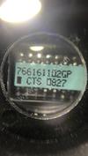
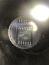
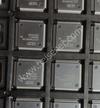
| Part Number | ICM7228AIPI |
|---|---|
| Manufacturer | Intersil |
| Description | IC DRIVER DECODER 8DIG 28DIP |
| Datasheet | |
| Package | 28-DIP (0.600", 15.24mm) |
| ECAD |
|
| In Stock | 6,832 piece(s) |
| Unit Price | Request a Quote |
| Lead Time | Can Ship Immediately |
| Estimated Delivery Time | Apr 28 - May 3 (Choose Expedited Shipping) |
| Request for Quotation |
|
| Payment Methods | |
| Delivery Services |
Part Number # ICM7228AIPI (PMIC - Display Drivers) is manufactured by Intersil and distributed by Heisener. Being one of the leading electronics distributors, we carry many kinds of electronic components from some of the world’s top class manufacturers. Their quality is guaranteed by its stringent quality control to meet all required standards.
For ICM7228AIPI specifications/configurations, quotation, lead time, payment terms of further enquiries please have no hesitation to contact us. To process your RFQ, please add ICM7228AIPI with quantity into BOM. Heisener.com does NOT require any registration to request a quote of ICM7228AIPI.
| Manufacturer | Intersil |
| Category | Integrated Circuits (ICs) - PMIC - Display Drivers |
| Package | 28-DIP (0.600", 15.24mm) |
| ECAD |
|
| Series | - |
| Display Type | LED |
| Configuration | 7 Segment |
| Interface | - |
| Digits or Characters | 8 Digits |
| Current - Supply | 200µA |
| Voltage - Supply | 4 V ~ 6 V |
| Operating Temperature | -40°C ~ 85°C |
| Mounting Type | Through Hole |
| Package / Case | 28-DIP (0.600", 15.24mm) |
| Supplier Device Package | 28-PDIP |
Kathe*****Carlson
March 24, 2023
Luk*****ennis
March 20, 2023
Sophi*****phens
March 19, 2023
Barr*****Mehra
March 12, 2023
Kane*****ierrez
March 8, 2023
Adal*****Conley
February 26, 2023
Euge*****ekhon
February 23, 2023


|
M39003/09-0076H | Vishay Sprague, CAP TANT 12UF 5% 50V AXIAL, Axial, - | View |

|
BD5351FVE-TR | Rohm Semiconductor, IC DETECTOR VOLT 5.1V CMOS 5VSOF, SOT-665, - | View |
 
|
L6392D | STMicroelectronics, IC DRIVER HV HI/LOW SIDE SOIC-14, 14-SOIC (0.154", 3.90mm Width), - | View |

|
P4SMA6.8A | Littelfuse Inc., TVS DIODE 5.8VWM 10.5VC SMD, DO-214AC, SMA, - | View |
|
|
0NLS225.X | Littelfuse Inc., FUSE CRTRDGE 225A 600VAC/500VDC, Cylindrical, Blade Terminals, - | View |

|
RNC55H2293BSB14 | Vishay Dale, RES 229K OHM 1/8W .1% AXIAL, Axial, - | View |

|
CRCW25122K74FKEGHP | Vishay Dale, RES SMD 2.74K OHM 1% 1.5W 2512, 2512 (6432 Metric), - | View |

|
RN73C1E71R5BTD | TE Connectivity Passive Product, RES SMD 71.5 OHM 0.1% 1/16W 0402, 0402 (1005 Metric), - | View |
|
|
1537-68G | API Delevan Inc., FIXED IND 68UH 176MA 3.3 OHM TH, Axial, - | View |
|
|
3213439 | Phoenix Contact, TERM BLOCK RCPT 7POS STR 3.5MM, -, - | View |

|
87916-422HLF | Amphenol FCI, HEADER BERGSTIK, -, - | View |
|
|
VG95234J2-10SL-3SN | ITT Cannon, LLC, CONN RCPT 3POS WALL MNT SKT, -, - | View |

We guarantee 100% customer satisfaction.
Our experienced sales team and tech support team back our services to satisfy all our customers.

We provide 90 days warranty.
If the items you received were not in perfect quality, we would be responsible for your refund or replacement, but the items must be returned in their original condition.
| Part Number | Manufacturer | Description | Stock |
ICM7228AIPI D# ICM7228AIPI |
Harris Semiconductor |
LED DRVR 64Segment 5V 28-Pin PDIP - Bulk (Alt: ICM7228AIPI) RoHS: Not Compliant
|
0 |
ICM7228AIPIZ D# ICM7228AIPIZ |
Intersil Corporation |
LED DRVR 64Segment 5V 28-Pin PDIP - Rail/Tube (Alt: ICM7228AIPIZ) RoHS: Compliant
|
0 |
| Part Number | Manufacturer | Description | Stock |
ICM7228AIPIZ D# ICM7228AIPIZ |
Renesas Electronics Corporation |
LED DRVR 64Segment 5V 28-Pin PDIP (Alt: ICM7228AIPIZ) RoHS: Compliant
|
0 |
| Part Number | Manufacturer | Description | Stock |
ICM7228AIPI |
Intersil Corporation | 14 | |
ICM7228AIPIZ |
Intersil Corporation | 9 |
| Part Number | Manufacturer | Description | Stock |
ICM7228AIPI |
Intersil Corporation |
LED DRIVER MUX 8 DIGIT, 7228, DIP28 |
295 |
ICM7228AIPIZ |
Intersil Corporation |
LED DRIVER MUX 8 DIGIT, 7228, DIP28 |
295 |
| Part Number | Manufacturer | Description | Stock |
ICM7228AIPIZ D# ICM7228AIPIZ-ND |
Renesas Electronics Corporation |
IC DRVR 7 SEGMENT 8 DIGIT 28DIP |
0 |
| Part Number | Manufacturer | Description | Stock |
ICM7228AIPI D# ICM7228AIPI |
Intersil Corporation |
Industry Leading ISO:9001/AS9120A Stocking Distributor of Obsolete & Hard to Find IC's/Semi's, Specializing in Altera/Xilinx. In-House Counterfeit Detection Lab. In Business 20 Years. Free Shipping on Orders Over $250. Buy American, Buy Direct |
1797 |
ICM7228AIPIZ D# ICM7228AIPIZ |
Intersil Corporation |
Industry Leading ISO:9001/AS9120A Stocking Distributor of Obsolete & Hard to Find IC's/Semi's, Specializing in Altera/Xilinx. In-House Counterfeit Detection Lab. In Business 20 Years. Free Shipping on Orders Over $250. Buy American, Buy Direct |
1504 |
| Part Number | Manufacturer | Description | Stock |
ICM7228AIPIZ |
Intersil Corporation |
In stock shipping within 2days |
500 |
ICM7228AIPI |
Intersil Corporation |
In stock shipping within 2days |
142 |
| Part Number | Manufacturer | Description | Stock |
ICM7228AIPIZ D# 1018168 |
Renesas Electronics Corporation |
LED DRIVER MUX 8 DIGIT, 7228, DIP28 RoHS: Compliant
Min Qty: 1
Container: Each
|
670 |
| Part Number | Manufacturer | Description | Stock |
ICM7228AIPI |
Renesas Electronics Corporation |
Available |
16500 |
| Part Number | Manufacturer | Description | Stock |
ICM7228AIPIZ |
Renesas Electronics Corporation |
ICM7228 Series 4 - 6 V 8-Digit LED Multiplexed Display Decoder Driver - PDIP-28 RoHS: Compliant
pbFree: Yes
|
201 |
| Part Number | Manufacturer | Description | Stock |
ICM7228AIPIZ |
Renesas Electronics Corporation |
OEM/CM QUOTES ONLY | NO BROKERS |
871 |
2ICM7228AIPIZ |
ITS |
OEM/CM QUOTES ONLY | NO BROKERS |
51 |
ICM7228AIPI |
Intersil Corporation |
OEM/CM QUOTES ONLY | NO BROKERS |
2320 |
| Part Number | Manufacturer | Description | Stock |
ICM7228AIPIZ |
Intersil Corporation |
In Stock |
9 |
| Part Number | Manufacturer | Description | Stock |
ICM7228AIPIZ |
Intersil Corporation |
in stock - can ship the same day |
43 |
| Part Number | Manufacturer | Description | Stock |
ICM7228AIPI |
Intersil Corporation |
OEM/CM Immediate delivery |
42 |
| Part Number | Manufacturer | Description | Stock |
ICM7228AIPIZ D# XSFP00000197747 |
Renesas Electronics Corporation |
ICM7228 Series 4 - 6 V 8-Digit LED Multiplexed Display Decoder Driver - PDIP-28 |
109 |
| Part Number | Manufacturer | Description | Stock |
ICM7228AIPIZ D# 97K1858 |
Renesas Electronics Corporation |
LED DRIVER MUX 8 DIGIT, 7228, DIP28, Device Topology:-, Input Voltage Min:4V, Input Voltage Max:6V, Output Voltage Max:5V, Output Current Max:100mA, Switching Frequency:-, No. of Outputs:16Outputs, IC Mounting:Through Hole, Driver RoHS Compliant: Yes RoHS: Compliant
Min Qty: 1
Container: Bulk
|
15 |
| Part Number | Manufacturer | Description | Stock |
ICM7228AIPIZ D# NS-ICM7228AIPIZ |
Intersil Corporation |
OEM/CM ONLY |
8167 |
| Part Number | Manufacturer | Description | Stock |
ICM7228AIPI |
Intersil Corporation |
LED DISPLAY DRIVER, 7-SEG, COMMON-ANODE, 28 Pin, Plastic, DIP |
11 |
ICM7228AIPIZ |
Intersil Corporation |
LED DRIVER, 7-SEGMENT, CMOS, PDIP28 |
33 |
| Part Number | Manufacturer | Description | Stock |
ICM7228AIPI |
Harris Semiconductor |
ICM7228 8-Digit, Microprocessor-Compatible, LED Display Decoder/Driver RoHS: Not Compliant
|
1289 |
| Part Number | Manufacturer | Description | Stock |
ICM7228AIPIZ D# ICPWM6094 |
Intersil Corporation |
LCDDr 8Digit PDIP-28 RoHS: Compliant
|
0 |
| Part Number | Manufacturer | Description | Stock |
ICM7228AIPI |
Intersil Corporation |
OEM/CM ONLY |
147 |
ICM7228AIPIZ |
Intersil Corporation |
OEM/CM ONLY |
299 |
2ICM7228AIPIZ |
ITS Electronics Inc |
OEM/CM ONLY |
140 |
| Part Number | Manufacturer | Description | Stock |
ICM7228AIPI |
Intersil Corporation |
IN stock Immediate delivery |
37 |
| Part Number | Manufacturer | Description | Stock |
ICM7228AIPI |
Intersil Corporation |
shipping today |
10144 |
ICM7228AIPIZ |
Intersil Corporation |
shipping today |
74 |
| Part Number | Manufacturer | Description | Stock |
ICM7228AIPI |
Intersil Corporation |
RFQ |
2366 |
ICM7228AIPIZ |
Intersil Corporation |
RFQ |
9583 |
| Part Number | Manufacturer | Description | Stock |
ICM7228AIPIZ D# 1018168 |
Renesas Electronics Corporation |
LED DRIVER MUX 8 DIGIT, 7228, DIP28 RoHS: Compliant
Min Qty: 1
Container: Each
|
742 |
Heisener's commitment to quality has shaped our processes for sourcing, testing, shipping, and every step in between. This foundation underlies each component we sell.

Do you have any question about ICM7228AIPI?
+86-755-83210559 ext. 815


Scan to view this page