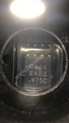
| Part Number | IXDI404PI |
|---|---|
| Manufacturer | IXYS |
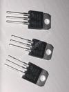
| Description | IC MOSFET DRIVER LS 4A DUAL 8DIP |
| Datasheet | |
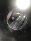
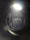
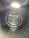
| Package | 8-DIP (0.300", 7.62mm) |
| ECAD |
|
| In Stock | 24,060 piece(s) |
| Unit Price | Request a Quote |
| Lead Time | Can Ship Immediately |
| Estimated Delivery Time | Apr 28 - May 3 (Choose Expedited Shipping) |
| Request for Quotation |
|
| Payment Methods | |
| Delivery Services |
Part Number # IXDI404PI (PMIC - Gate Drivers) is manufactured by IXYS and distributed by Heisener. Being one of the leading electronics distributors, we carry many kinds of electronic components from some of the world’s top class manufacturers. Their quality is guaranteed by its stringent quality control to meet all required standards.
For IXDI404PI specifications/configurations, quotation, lead time, payment terms of further enquiries please have no hesitation to contact us. To process your RFQ, please add IXDI404PI with quantity into BOM. Heisener.com does NOT require any registration to request a quote of IXDI404PI.
| Manufacturer | IXYS |
| Category | Integrated Circuits (ICs) - PMIC - Gate Drivers |
| Package | 8-DIP (0.300", 7.62mm) |
| ECAD |
|
| Series | - |
| Driven Configuration | Low-Side |
| Channel Type | Independent |
| Number of Drivers | 2 |
| Gate Type | IGBT, N-Channel, P-Channel MOSFET |
| Voltage - Supply | 4.5 V ~ 35 V |
| Logic Voltage - VIL, VIH | 0.8V, 2.5V |
| Current - Peak Output (Source, Sink) | 4A, 4A |
| Input Type | Inverting |
| High Side Voltage - Max (Bootstrap) | - |
| Rise / Fall Time (Typ) | 16ns, 13ns |
| Operating Temperature | -55°C ~ 150°C (TJ) |
| Mounting Type | Through Hole |
| Package / Case | 8-DIP (0.300", 7.62mm) |
| Supplier Device Package | 8-PDIP |
Henl*****oshi
April 1, 2023
Noe*****yal
March 25, 2023
Jenny*****dhury
March 18, 2023
Josl*****ierra
March 17, 2023
Rache*****shall
March 15, 2023
Toma*****octor
March 7, 2023
Evaly*****ffith
February 26, 2023
Zaniy*****uilar
February 20, 2023


|
SIT8209AI-G3-33E-156.257812Y | SiTIME, -40 TO 85C, 2520, 50PPM, 3.3V, 1, -, - | View |
|
|
VJ0805D271FXBAT | Vishay Vitramon, CAP CER 270PF 100V NP0 0805, 0805 (2012 Metric), - | View |

|
1206J5000391KDR | Knowles Syfer, CAP CER 390PF 500V X7R 1206, 1206 (3216 Metric), - | View |

|
K821K15C0GK53L2 | Vishay BC Components, CAP CER 820PF 200V C0G/NP0 RAD, Radial, - | View |

|
UPJ1J390MED1TA | Nichicon, CAP ALUM 39UF 20% 63V RADIAL, Radial, Can, - | View |
|
|
8N3DV85AC-0043CDI8 | IDT, Integrated Device Technology Inc, IC OSC VCXO DUAL FREQ 6-CLCC, 6-CLCC, - | View |
|
|
KR HAVPA1.22-VWAV-DQ-20-R33-Z | OSRAM Opto Semiconductors Inc., DISPLIX OVAL RED, 1008 (2721 Metric), - | View |

|
MCR100JZHJLR15 | Rohm Semiconductor, RES SMD 0.15 OHM 5% 1W 2512, 2512 (6432 Metric), - | View |
|
|
DW-20-15-T-D-363 | Samtec Inc., .025" BOARD SPACERS, -, - | View |
|
|
SBC9110 | Winchester Electronics, CONN BNC PLUG STR 75 OHM CRIMP, -, - | View |
|
|
PT06E-22-34P | Amphenol Industrial Operations, CONN PLUG 34POS INLINE PIN, -, - | View |
|
|
VE-B3B-EW-F3 | Vicor Corporation, CONVERTER MOD DC/DC 95V 100W, Full Brick, - | View |

We guarantee 100% customer satisfaction.
Our experienced sales team and tech support team back our services to satisfy all our customers.

We provide 90 days warranty.
If the items you received were not in perfect quality, we would be responsible for your refund or replacement, but the items must be returned in their original condition.
| Part Number | Manufacturer | Description | Stock |
IXDI404PI |
IXYS Corporation |
IC MOSFET DRIVER LS 4A DUAL 8DIP |
0 |
| Part Number | Manufacturer | Description | Stock |
IXDI404PI |
IXYS Corporation |
OEM/CM QUOTES ONLY | NO BROKERS |
580 |
| Part Number | Manufacturer | Description | Stock |
IXDI404PI |
IXYS Corporation |
OEM/CM Immediate delivery |
186 |
| Part Number | Manufacturer | Description | Stock |
IXDI404PI D# NS-IXDI404PI |
IXYS Corporation |
OEM/CM ONLY |
6921 |
| Part Number | Manufacturer | Description | Stock |
IXDI 404PI |
IXYS Corporation |
OEM/CM ONLY |
66 |
| Part Number | Manufacturer | Description | Stock |
IXDI404PI |
IXYS Corporation |
IN stock Immediate delivery |
181 |
Heisener's commitment to quality has shaped our processes for sourcing, testing, shipping, and every step in between. This foundation underlies each component we sell.

Do you have any question about IXDI404PI?
+86-755-83210559-810


Scan to view this page