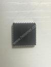
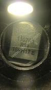
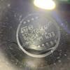
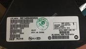
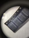
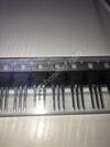
Part Number | KA7806ETU |
---|---|
Manufacturer | Fairchild/ON Semiconductor |
Description | IC REG LINEAR 6V 1A TO220-3 |
Datasheet | KA7806ETU Datasheet |
Package | TO-220-3 |
In Stock | 18,020 piece(s) |
Unit Price | $ 0.6000 * |
Lead Time | Can Ship Immediately |
Estimated Delivery Time | Jan 24 - Jan 29 (Choose Expedited Shipping) |
Request for Quotation |
|
Part Number # KA7806ETU (PMIC - Voltage Regulators - Linear) is manufactured by Fairchild/ON Semiconductor and distributed by Heisener. Being one of the leading electronics distributors, we carry many kinds of electronic components from some of the world’s top class manufacturers. Their quality is guaranteed by its stringent quality control to meet all required standards.
For KA7806ETU specifications/configurations, quotation, lead time, payment terms of further enquiries please have no hesitation to contact us. To process your RFQ, please add KA7806ETU with quantity into BOM. Heisener.com does NOT require any registration to request a quote of KA7806ETU.
Manufacturer | Fairchild/ON Semiconductor |
Category | Integrated Circuits (ICs) - PMIC - Voltage Regulators - Linear |
Datasheet | KA7806ETUDatasheet |
Package | TO-220-3 |
Series | - |
Output Configuration | Positive |
Output Type | Fixed |
Number of Regulators | 1 |
Voltage - Input (Max) | 35V |
Voltage - Output (Min/Fixed) | 6V |
Voltage - Output (Max) | - |
Voltage Dropout (Max) | 2V @ 1A (Typ) |
Current - Output | 1A |
Current - Quiescent (Iq) | - |
Current - Supply (Max) | 8mA |
PSRR | 75dB (120Hz) |
Control Features | - |
Protection Features | Over Temperature, Short Circuit |
Operating Temperature | -40°C ~ 125°C |
Mounting Type | Through Hole |
Package / Case | TO-220-3 |
Supplier Device Package | TO-220-3 |
To learn more about ON Semiconductor, please visit our website at www.onsemi.com Please note: As part of the Fairchild Semiconductor integration, some of the Fairchild orderable part numbers will need to change in order to meet ON Semiconductor’s system requirements. Since the ON Semiconductor product management systems do not have the ability to manage part nomenclature that utilizes an underscore (_), the underscore (_) in the Fairchild part numbers will be changed to a dash (-). This document may contain device numbers with an underscore (_). Please check the ON Semiconductor website to verify the updated device numbers. The most current and up-to-date ordering information can be found at www.onsemi.com. Please email any questions regarding the system integration to Fairchild_questions@onsemi.com. Is Now Part of ON Semiconductor and the ON Semiconductor logo are trademarks of Semiconductor Components Industries, LLC dba ON Semiconductor or its subsidiaries in the United States and/or other countries. ON Semiconductor owns the rights to a number of patents, trademarks, copyrights, trade secrets, and other intellectual property. A listing of ON Semiconductor’s product/patent coverage may be accessed at www.onsemi.com/site/pdf/Patent-Marking.pdf. ON Semiconductor reserves the right to make changes without further notice to any products herein. ON Semiconductor makes no warranty, representation or guarantee regarding the suitability of its products for any particular purpose, nor does ON Semiconductor assume any liability arising out of the application or use of any product or circuit, and specifically disclaims any and all liability, including without limitation special, consequential or incidental damages. Buyer is responsible for its products and applications using ON Semiconductor products, including compliance with all laws, regulations and safety requirements or standards, regardless of any support or applications information provided by ON Semiconductor. “Typical” parameters which may be provided in ON Semiconductor data sheets and/or specifications can and do vary in different applications and actual performance may vary over time. All operating parameters, including “Typicals” must be validated for each customer application by customer’s technical experts. ON Semiconductor does not convey any license under its patent rights nor the rights of others. ON Semiconductor products are not designed, intended, or authorized for use as a critical component in life support systems or any FDA Class 3 medical devices or medical devices with a same or similar classification in a foreign jurisdiction or any devices intended for implantation in the human body. Should Buyer purchase or use ON Semiconductor products for any such unintended or unauthorized application, Buyer shall indemnify and hold ON Semiconductor and its officers, employees, subsidiaries, affiliates, and distributors harmless against all claims, costs, damages, and expenses, and reasonable attorney fees arising out of, directly or indirectly, any claim of personal injury or death associated with such unintended or unauthorized use, even if such claim alleges that ON Semiconductor was negligent regarding the design or manufacture of the part. ON Semiconductor is an Equal Opportunity/Affirmative Action Employer. This literature is subject to all applicable copyright laws and is not for resale in any manner.
K A 78X X E / K A 78X X A E — 3-Term in al 1 A P o sitive V o ltag e R eg u lato r © 2006 Fairchild Semiconductor Corporation www.fairchildsemi.com KA78XXE / KA78XXAE Rev. 1.9 April 2015 KA78XXE / KA78XXAE 3-Terminal 1 A Positive Voltage Regulator Features • Output Current up to 1 A • Output Voltages of 5, 6, 8, 9, 10, 12, 15, 18, 24 V • Thermal Overload Protection • Short-Circuit Protection • Output Transistor Safe Operating Area Protection Block Diagram Figure 1. Block Diagram SERIES PASS ELEMENT SOA PROTECTION ERROR AMPLIFIER THERMAL PROTECTION CURRENT GENERATOR REFERENCE VOLTAGE STARTING CIRCUIT OUTPUT 3 GND 2 INPUT 1 Description The KA78XXE / KA78XXAE series of three-terminal posi- tive regulators is available in the TO-220 / D-PAK pack- age with several fixed-output voltages, making them useful in a wide range of applications. Each type employs internal current limiting, thermal shut-down, and safe operating area. If adequate heat sinking is provided, they can deliver over 1 A output current. Although designed primarily as fixed-voltage regulators, these devices can be used with external components for adjustable voltages and currents. 1 1. Input 2. GND 3. Output 1 GND TO-220 D-PAK GND (Dual Gauge)
K A 78X X E / K A 78X X A E — 3-Term in al 1 A P o sitive V o ltag e R eg u lato r © 2006 Fairchild Semiconductor Corporation www.fairchildsemi.com KA78XXE / KA78XXAE Rev. 1.9 2 Ordering Information Notes: 1. Above output voltage tolerance is available at 25°C. 2. Refer to below figure for TM / TF Suffix for DPAK. Product Number Output Voltage Tolerance(1) Package Operating Temperature Parking Method KA7805ETU ±4% TO-220 (Dual Gauge) -40°C to +125°C Rail KA7806ETU KA7808ETU KA7809ETU KA7810ETU KA7812ETU KA7815ETU KA7818ETU KA7824ETU KA7805ERTF D-PAK(2) Tape and Reel KA7805ERTM KA7808ERTM KA7809ERTM KA7812ERTM KA7805AETU ±2% TO-220 (Dual Gauge) 0°C to +125°C Rail KA7809AETU KA7810AETU KA7812AETU KA7815AETU KA7824AETU
K A 78X X E / K A 78X X A E — 3-Term in al 1 A P o sitive V o ltag e R eg u lato r © 2006 Fairchild Semiconductor Corporation www.fairchildsemi.com KA78XXE / KA78XXAE Rev. 1.9 3 Absolute Maximum Ratings Stresses exceeding the absolute maximum ratings may damage the device. The device may not function or be opera- ble above the recommended operating conditions and stressing the parts to these levels is not recommended. In addi- tion, extended exposure to stresses above the recommended operating conditions may affect device reliability. The absolute maximum ratings are stress ratings only. Values are at TA = 25°C unless otherwise noted. Symbol Parameter Value Unit VI Input Voltage VO = 5 V to 18 V 35 V VO = 24 V 40 V RθJC Thermal Resistance Junction-Case (TO-220) 5 °C/W RθJA Thermal Resistance Junction-Air (TO-220) 65 °C/W TOPR Operating Temperature Range KA78XXE / KA78XXER -40 to +125 °C KA78XXAE 0 to +125 TSTG Storage Temperature Range -65 to +150 °C
K A 78X X E / K A 78X X A E — 3-Term in al 1 A P o sitive V o ltag e R eg u lato r © 2006 Fairchild Semiconductor Corporation www.fairchildsemi.com KA78XXE / KA78XXAE Rev. 1.9 4 Electrical Characteristics (KA7805E / KA7805ER) Refer to test circuit, -40°C < TJ < 125°C, IO = 500 mA, VI =10 V, CI= 0.33 μF, CO=0.1 μF, unless otherwise specified. Notes: 3. Load and line regulation are specified at constant junction temperature. Changes in VO due to heating effects must be taken into account separately. Pulse testing with low duty is used. 4. These parameters, although guaranteed, are not 100% tested in production. Symbol Parameter Conditions Min. Typ. Max. Unit VO Output Voltage TJ = +25°C 4.80 5.00 5.20 V5.0 mA ≤ IO ≤1.0 A, PO ≤15 W, VI = 7 V to 20 V 4.75 5.00 5.25 Regline Line Regulation(3) TJ = +25°C VI = 7 V to 25 V 4.0 100.0 mV VI = 8 V to 12 V 1.6 50.0 Regload Load Regulation(3) TJ = +25°C IO = 5.0 mA to 1.5 A 9 100 mV IO = 250 mA to 750 mA 4 50 IQ Quiescent Current TJ = +25°C 5 8 mA ΔIQ Quiescent Current Change IO = 5 mA to 1.0 A 0.03 0.50 mA VI = 7 V to 25 V 0.30 1.30 ΔVO/ΔT Output Voltage Drift (4) IO = 5 mA -0.8 mV/°C VN Output Noise Voltage f = 10 Hz to 100 kHz, TA = +25°C 42 μV RR Ripple Rejection(4) f = 120 Hz, VI = 8 V to 18 V 62 73 dB VDrop Dropout Voltage IO = 1 A, TJ = +25°C 2 V RO Output Resistance (4) f = 1 kHz 15 mΩ ISC Short-Circuit Current VI = 35 V, TA = +25°C 230 mA IPK Peak Current (4) TJ = +25°C 2.2 A
K A 78X X E / K A 78X X A E — 3-Term in al 1 A P o sitive V o ltag e R eg u lato r © 2006 Fairchild Semiconductor Corporation www.fairchildsemi.com KA78XXE / KA78XXAE Rev. 1.9 5 Electrical Characteristics (KA7806E) Refer to test circuit, -40°C < TJ < 125°C, IO = 500 mA, VI = 11 V, CI = 0.33 μF, CO = 0.1 μF, unless otherwise specified. Notes: 5. Load and line regulation are specified at constant junction temperature. Changes in VO due to heating effects must be taken into account separately. Pulse testing with low duty is used. 6. These parameters, although guaranteed, are not 100% tested in production. Symbol Parameter Conditions Min. Typ. Max. Unit VO Output Voltage TJ = +25°C 5.75 6.00 6.25 V5.0 mA ≤ IO ≤1.0 A, PO ≤15 W, VI = 8.0 V to 21 V 5.70 6.00 6.30 Regline Line Regulation(5) TJ = +25°C VI = 8 V to 25 V 5.0 120.0 mV VI = 9 V to 13 V 1.5 60.0 Regload Load Regulation(5) TJ = +25°C IO = 5 mA to 1.5 A 9 120 mV IO = 250 mA to 750 mA 3 60 IQ Quiescent Current TJ = +25°C 5 8 mA ΔIQ Quiescent Current Change IO = 5 mA to 1 A 0.5 mA VI = 8 V to 25 V 1.3 ΔVO/ΔT Output Voltage Drift (6) IO = 5 mA -0.8 mV/°C VN Output Noise Voltage f = 10 Hz to 100 kHz, TA = +25°C 45 μV RR Ripple Rejection(6) f = 120 Hz, VI = 9 V to 19 V 59 75 dB VDrop Dropout Voltage IO = 1 A, TJ = +25°C 2 V RO Output Resistance (6) f = 1 kHz 19 mΩ ISC Short-Circuit Current VI = 35 V, TA= +25°C 250 mA IPK Peak Current (6) TJ = +25°C 2.2 A
K A 78X X E / K A 78X X A E — 3-Term in al 1 A P o sitive V o ltag e R eg u lato r © 2006 Fairchild Semiconductor Corporation www.fairchildsemi.com KA78XXE / KA78XXAE Rev. 1.9 6 Electrical Characteristics (KA7808E / KA7808ER) Refer to test circuit, -40°C < TJ < 125°C, IO = 500 mA, VI = 14 V, CI = 0.33 μF, CO = 0.1 μF, unless otherwise specified. Notes: 7. Load and line regulation are specified at constant junction temperature. Changes in VO due to heating effects must be taken into account separately. Pulse testing with low duty is used. 8. These parameters, although guaranteed, are not 100% tested in production. Symbol Parameter Conditions Min. Typ. Max. Unit VO Output Voltage TJ = +25°C 7.7 8.0 8.3 V5.0 mA ≤ IO ≤1.0 A, PO ≤15 W, VI = 10.5 V to 23 V 7.6 8.0 8.4 Regline Line Regulation(7) TJ = +25°C VI = 10.5 V to 25 V 5 160 mV VI = 11.5 V to 17 V 2 80 Regload Load Regulation(7) TJ = +25°C IO = 5.0 mA to 1.5 A 10 160 mV IO = 250 mA to 750 mA 5 80 IQ Quiescent Current TJ = +25°C 5 8 mA ΔIQ Quiescent Current Change IO = 5 mA to 1.0 A 0.05 0.50 mA VI = 10.5 A to 25 V 0.50 1.00 ΔVO/ΔT Output Voltage Drift (8) IO = 5 mA -0.8 mV/°C VN Output Noise Voltage f = 10 Hz to 100 kHz, TA = +25°C 52 μV RR Ripple Rejection(8) f = 120 Hz, VI= 11.5 V to 21.5 V 56 73 dB VDrop Dropout Voltage IO = 1 A, TJ = +25°C 2 V RO Output Resistance (8) f = 1 kHz 17 mΩ ISC Short-Circuit Current VI = 35 V, TA = +25°C 230 mA IPK Peak Current (8) TJ = +25°C 2.2 A
K A 78X X E / K A 78X X A E — 3-Term in al 1 A P o sitive V o ltag e R eg u lato r © 2006 Fairchild Semiconductor Corporation www.fairchildsemi.com KA78XXE / KA78XXAE Rev. 1.9 7 Electrical Characteristics (KA7809E / KA7809ER) Refer to test circuit, -40°C < TJ < 125°C, IO = 500 mA, VI = 15 V, CI = 0.33 μF, CO = 0.1 μF, unless otherwise specified. Notes: 9. Load and line regulation are specified at constant junction temperature. Changes in VO due to heating effects must be taken into account separately. Pulse testing with low duty is used. 10. These parameters, although guaranteed, are not 100% tested in production. Symbol Parameter Conditions Min. Typ. Max. Unit VO Output Voltage TJ = +25°C 8.65 9.00 9.35 V5.0 mA ≤ IO ≤ 1.0 A, PO ≤ 15 W, VI = 11.5 V to 24 V 8.60 9.00 9.40 Regline Line Regulation(9) TJ = +25°C VI = 11.5 V to 25 V 6 180 mV VI = 12 V to 17 V 2 90 Regload Load Regulation(9) TJ = +25°C IO = 5 mA to 1.5 A 12 180 mV IO = 250 mA to 750 mA 4 90 IQ Quiescent Current TJ = +25°C 5 8 mA ΔIQ Quiescent Current Change IO = 5 mA to 1.0 A 0.5 mA VI = 11.5 V to 26 V 1.3 ΔVO/ΔT Output Voltage Drift (10) IO = 5 mA -1 mV/°C VN Output Noise Voltage f = 10 Hz to 100 kHz, TA = +25°C 58 μV RR Ripple Rejection(10) f = 120 Hz, VI = 13 V to 23 V 56 71 dB VDrop Dropout Voltage IO = 1 A, TJ = +25°C 2 V RO Output Resistance (10) f = 1 kHz 17 mΩ ISC Short-Circuit Current VI = 35 V, TA = +25°C 250 mA IPK Peak Current (10) TJ = +25°C 2.2 A
K A 78X X E / K A 78X X A E — 3-Term in al 1 A P o sitive V o ltag e R eg u lato r © 2006 Fairchild Semiconductor Corporation www.fairchildsemi.com KA78XXE / KA78XXAE Rev. 1.9 8 Electrical Characteristics (KA7810E) Refer to test circuit, -40°C < TJ < 125°C, IO = 500 mA, VI = 16 V, CI = 0.33 μF, CO = 0.1 μF, unless otherwise specified. Notes: 11. Load and line regulation are specified at constant junction temperature. Changes in VO due to heating effects must be taken into account separately. Pulse testing with low duty is used. 12. These parameters, although guaranteed, are not 100% tested in production. Symbol Parameter Conditions Min. Typ. Max. Unit VO Output Voltage TJ = +25°C 9.6 10.0 10.4 V5.0 mA ≤ IO ≤ 1.0 A, PO ≤ 15 W, VI = 12.5 V to 25 V 9.5 10.0 10.5 Regline Line Regulation(11) TJ = +25°C VI = 12.5 V to 25 V 10 200 mV VI = 13 V to 25 V 3 100 Regload Load Regulation(11) TJ = +25°C IO = 5 mA to 1.5 A 12 200 mV IO = 250 mA to 750 mA 4 400 IQ Quiescent Current TJ = +25°C 5.1 8.0 mA ΔIQ Quiescent Current Change IO = 5 mA to 1.0 A 0.5 mA VI = 12.5 V to 29 V 1.0 ΔVO/ΔT Output Voltage Drift (12) IO = 5 mA -1 mV/°C VN Output Noise Voltage f = 10 Hz to 100 kHz, TA = +25°C 58 μV RR Ripple Rejection(12) f = 120 Hz, VI = 13 V to 23 V 56 71 dB VDrop Dropout Voltage IO = 1 A, TJ = +25°C 2 V RO Output Resistance (12) f = 1 kHz 17 mΩ ISC Short-Circuit Current VI = 35 V, TA = +25°C 250 mA IPK Peak Current (12) TJ = +25°C 2.2 A
Shawn *****adhyay
December 27, 2021
Kell*****ierra
December 25, 2020
We guarantee 100% customer satisfaction.
Our experienced sales team and tech support team back our services to satisfy all our customers.
We provide 90 days warranty.
If the items you received were not in perfect quality, we would be responsible for your refund or replacement, but the items must be returned in their original condition.
Payment Methods | |
Delivery Services |
Heisener's commitment to quality has shaped our processes for sourcing, testing, shipping, and every step in between. This foundation underlies each component we sell.