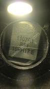
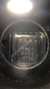
| Part Number | LD39200DPUR |
|---|---|
| Manufacturer | STMicroelectronics |
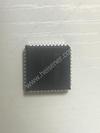
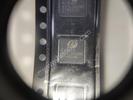
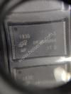
| Description | IC REG LINEAR POS ADJ 2A 8DFN |
| Datasheet | |
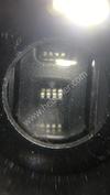
| Package | 8-VDFN Exposed Pad |
| ECAD |
|
| In Stock | 5,472 piece(s) |
| Unit Price | $ 1.3255 * |
| Lead Time | To be Confirmed |
| Estimated Delivery Time | Apr 27 - May 2 (Choose Expedited Shipping) |
| Request for Quotation |
|
| Payment Methods | |
| Delivery Services |
Part Number # LD39200DPUR (PMIC - Voltage Regulators - Linear) is manufactured by STMicroelectronics and distributed by Heisener. Being one of the leading electronics distributors, we carry many kinds of electronic components from some of the world’s top class manufacturers. Their quality is guaranteed by its stringent quality control to meet all required standards.
For LD39200DPUR specifications/configurations, quotation, lead time, payment terms of further enquiries please have no hesitation to contact us. To process your RFQ, please add LD39200DPUR with quantity into BOM. Heisener.com does NOT require any registration to request a quote of LD39200DPUR.
| Manufacturer | STMicroelectronics |
| Category | Integrated Circuits (ICs) - PMIC - Voltage Regulators - Linear |
| Package | 8-VDFN Exposed Pad |
| ECAD |
|
| Series | - |
| Output Configuration | Positive |
| Output Type | Adjustable |
| Number of Regulators | 1 |
| Voltage - Input (Max) | 6V |
| Voltage - Output (Min/Fixed) | 0.5V |
| Voltage - Output (Max) | 5.75V |
| Voltage Dropout (Max) | 0.25V @ 2A |
| Current - Output | 2A |
| Current - Quiescent (Iq) | - |
| Current - Supply (Max) | 300µA ~ 3mA |
| PSRR | 70dB ~ 40dB (1kHz ~ 1MHz) |
| Control Features | Enable, Power Good |
| Protection Features | Over Current, Over Temperature, Reverse Polarity |
| Operating Temperature | -40°C ~ 125°C |
| Mounting Type | Surface Mount |
| Package / Case | 8-VDFN Exposed Pad |
| Supplier Device Package | 8-DFN (4x4) |
Journ*****ntreras
March 28, 2023
Fabi*****alls
March 27, 2023
Zavier*****rishnan
March 15, 2023
Juli*****elps
March 4, 2023
Bria*****osas
February 28, 2023
Jord*****athak
February 24, 2023


|
SIT1602BC-71-33E-30.000000G | SiTIME, -20 TO 70C, 2016, 20PPM, 3.3V, 3, -, - | View |

|
7C-50.000MBB-T | TXC CORPORATION, OSC XO 50.000MHZ CMOS SMD, 4-SMD, No Lead, - | View |

|
CS325S-38.400MEEQ-UT | Citizen Finedevice Co Ltd, CRYSTAL 38.4000MHZ 10PF SMD, 4-SMD, No Lead, - | View |

|
2225J0160102GFR | Knowles Syfer, CAP CER 2225, -, - | View |

|
EGXF500ELL102MK30S | United Chemi-Con, CAP MINI ALUM ELECTRO, Radial, Can, - | View |
 
|
AD8042AR-REEL7 | Analog Devices Inc., IC OPAMP VFB 170MHZ RRO 8SOIC, 8-SOIC (0.154", 3.90mm Width), - | View |

|
XRCWHT-L1-R250-006B8 | Cree Inc., LED XLAMP WARM/NEUTRAL WHT 2SMD, 3529 (9073 Metric), - | View |
|
|
MY4-02-AC50 | Omron Automation and Safety, RELAY GEN PURPOSE 4PDT 3A 50V, -, - | View |
|
|
20020013-H241B01LF | Amphenol Anytek, TERM BLOCK PLUG 24POS STR 5.08MM, -, - | View |
|
|
3408-53K2UG | 3M, CONN HEADER 16POS R/A LONG LATCH, -, - | View |
|
|
CIR06AF-32A-5P | ITT Cannon, LLC, CONN PLUG 5POS STRGHT PIN, -, - | View |

|
REC3-4809SRW/H6/A/M/CTRL/X2 | Recom Power, DC/DC CONVERTER 9V 3W, 24-DIP Module, 8 Leads, - | View |

We guarantee 100% customer satisfaction.
Our experienced sales team and tech support team back our services to satisfy all our customers.

We provide 90 days warranty.
If the items you received were not in perfect quality, we would be responsible for your refund or replacement, but the items must be returned in their original condition.
| Part Number | Manufacturer | Description | Stock |
LD39200DPUR D# V72:2272_17745686 |
STMicroelectronics |
LDO Regulator Pos 0.5V 2A 8-Pin VFDFPN EP T/R RoHS: Compliant
|
0 |
| Part Number | Manufacturer | Description | Stock |
LD39200DPUR D# LD39200DPUR |
STMicroelectronics |
2A high PSRR ultra low drop (LDO) linear regulator - Tape and Reel (Alt: LD39200DPUR) |
0 |
| Part Number | Manufacturer | Description | Stock |
LD39200DPUR D# LD39200DPUR |
STMicroelectronics |
2A high PSRR ultra low drop (LDO) linear regulator (Alt: LD39200DPUR) |
0 |
| Part Number | Manufacturer | Description | Stock |
LD39200DPUR D# LD39200DPUR |
STMicroelectronics |
2A high PSRR ultra low drop (LDO) linear regulator (Alt: LD39200DPUR) |
0 |
| Part Number | Manufacturer | Description | Stock |
LD39200DPUR |
STMicroelectronics |
DFN-8 Dropout Regulators(LDO) RoHS |
4033 |
| Part Number | Manufacturer | Description | Stock |
LD39200DPUR D# 497-14961-1-ND |
STMicroelectronics |
IC REG LINEAR POS ADJ 2A 8DFN |
2653 |
| Part Number | Manufacturer | Description | Stock |
LD39200DPUR |
STMicroelectronics |
In stock shipping within 2days |
9260 |
| Part Number | Manufacturer | Description | Stock |
LD39200DPUR D# 2849786 |
STMicroelectronics |
LDO, ADJ, 1.5V, 0.3A, TSOP-5 RoHS: Compliant
Min Qty: 1
Container: Each
|
832 |
| Part Number | Manufacturer | Description | Stock |
LD39200DPUR |
STMicroelectronics |
LD39200 Series 2 A ADJ Output High PSRR Ultra LDO Linear Regulator- DFN-8 (4x4) RoHS: Compliant
pbFree: Yes
|
4500 |
| Part Number | Manufacturer | Description | Stock |
LD39200DPUR |
STMicroelectronics |
OEM/CM QUOTES ONLY | NO BROKERS |
34800 |
| Part Number | Manufacturer | Description | Stock |
LD39200DPUR D# C880590 |
STMicroelectronics | 4033 |
| Part Number | Manufacturer | Description | Stock |
LD39200DPUR |
STMicroelectronics |
OEM/CM Immediate delivery |
30000 |
| Part Number | Manufacturer | Description | Stock |
LD39200DPUR D# 511-LD39200DPUR |
STMicroelectronics |
LDO Voltage Regulators POWER MANAGEMENT RoHS: Compliant
|
3854 |
| Part Number | Manufacturer | Description | Stock |
LD39200DPUR D# XSFP00000086597 |
STMicroelectronics |
LD39200 Series 2 A ADJ Output High PSRR Ultra LDO Linear Regulator - DFN-8 (4x4) |
9000 |
| Part Number | Manufacturer | Description | Stock |
LD39200DPUR D# 51AC9078 |
STMicroelectronics |
LDO, ADJ, 1.5V, 0.3A, TSOP-5, Output Type:Adjustable, Input Voltage Min:1.25V, Input Voltage Max:6V, Fixed Output Voltage Nom.:-, Adjustable Output Voltage Min:500mV, Adjustable Output Voltage Max:750mV, Output Current:2A, Dropout RoHS Compliant: Yes RoHS: Compliant
Min Qty: 1
Container: Bulk
|
697 |
| Part Number | Manufacturer | Description | Stock |
LD39200DPUR D# 1961949 |
STMicroelectronics |
STMicroelectronics LD39200DPUR, LDO Voltage Regulator, 2A Adjustable, 0.8 4.5 V, 3% 8-Pin, DFN, RL Min Qty: 4500
Container: Reel
|
3100 |
| Part Number | Manufacturer | Description | Stock |
LD39200DPUR |
STMicroelectronics |
OEM/CM ONLY |
101 |
| Part Number | Manufacturer | Description | Stock |
LD39200DPUR |
STMicroelectronics |
IN stock Immediate delivery |
29985 |
| Part Number | Manufacturer | Description | Stock |
LD39200DPUR |
STMicroelectronics |
shipping today |
609 |
| Part Number | Manufacturer | Description | Stock |
LD39200DPUR D# 50476646 |
STMicroelectronics |
LDO Regulator Pos 0.5V 2A 8-Pin VFDFPN EP T/R RoHS: Compliant
|
0 |
| Part Number | Manufacturer | Description | Stock |
LD39200DPUR D# 2849786 |
STMicroelectronics |
LDO, ADJ, 1.5V, 0.3A, TSOP-5 RoHS: Compliant
Min Qty: 1
Container: Each
|
1147 |
Heisener's commitment to quality has shaped our processes for sourcing, testing, shipping, and every step in between. This foundation underlies each component we sell.

Do you have any question about LD39200DPUR?
+86-755-83210559-827


Scan to view this page