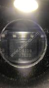
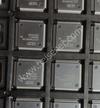
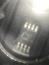
| Part Number | LED1642GWTTR |
|---|---|
| Manufacturer | STMicroelectronics |
| Description | IC LED DRVR LIN DIM 40MA 24TSSOP |
| Datasheet | |
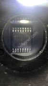
| Package | 24-TSSOP (0.173", 4.40mm Width) |
| ECAD |
|
| In Stock | 14,604 piece(s) |
| Unit Price | $ 2.5658 * |
| Lead Time | Can Ship Immediately |
| Estimated Delivery Time | Apr 21 - Apr 26 (Choose Expedited Shipping) |
| Request for Quotation |
|
| Payment Methods | |
| Delivery Services |
Part Number # LED1642GWTTR (PMIC - LED Drivers) is manufactured by STMicroelectronics and distributed by Heisener. Being one of the leading electronics distributors, we carry many kinds of electronic components from some of the world’s top class manufacturers. Their quality is guaranteed by its stringent quality control to meet all required standards.
For LED1642GWTTR specifications/configurations, quotation, lead time, payment terms of further enquiries please have no hesitation to contact us. To process your RFQ, please add LED1642GWTTR with quantity into BOM. Heisener.com does NOT require any registration to request a quote of LED1642GWTTR.
| Manufacturer | STMicroelectronics |
| Category | Integrated Circuits (ICs) - PMIC - LED Drivers |
| Package | 24-TSSOP (0.173", 4.40mm Width) |
| ECAD |
|
| Series | - |
| Type | Linear |
| Topology | Shift Register |
| Internal Switch(s) | Yes |
| Number of Outputs | 16 |
| Voltage - Supply (Min) | 3V |
| Voltage - Supply (Max) | 5.5V |
| Voltage - Output | 19V |
| Current - Output / Channel | 40mA |
| Frequency | 30MHz |
| Dimming | PWM |
| Applications | Signage |
| Operating Temperature | -40°C ~ 85°C (TA) |
| Mounting Type | Surface Mount |
| Package / Case | 24-TSSOP (0.173", 4.40mm Width) |
| Supplier Device Package | 24-TSSOP |
Emma*****Mand
April 5, 2023
Manu*****hakkar
March 27, 2023
Pablo*****raborty
March 9, 2023
Fletc*****hetty
March 3, 2023
Gene*****Casey
March 2, 2023
Scar***** Dixit
February 20, 2023


|
SIT8208AC-8F-18S-74.176000T | SiTIME, -20 TO 70C, 7050, 10PPM, 1.8V, 7, -, - | View |

|
2EZ160D10/TR8 | Microsemi Corporation, DIODE ZENER 160V 2W DO204AL, DO-204AL, DO-41, Axial, - | View |

|
BD50GA3WEFJ-E2 | Rohm Semiconductor, IC REG LINEAR 5V 300MA 8HTSOP-J, 8-SOIC (0.154", 3.90mm Width) Exposed Pad, - | View |
 
|
STA308 | STMicroelectronics, IC AUDIO PROCESSOR DGTL 64-TQFP, 64-LQFP, - | View |

|
E6A2CS3C 200P/R 0.5M | Omron Automation and Safety, ENCODER ROTARY 5-12V 200RES .5M, -, - | View |
|
|
RWR80S6650FRRSL | Vishay Dale, RES 665 OHM 2W 1% WW AXIAL, Axial, - | View |

|
RSMF12JB20R0 | Stackpole Electronics Inc., RES 20 OHM 1/2W 5% AXIAL, Axial, - | View |
|
|
BCS-104-SM-D-DE-BE | Samtec Inc., BOX CONNECTOR SOCKET STRIP, -, - | View |

|
1-102617-8 | TE Connectivity AMP Connectors, CONN HEADER R/A .100 40POS 15AU, -, - | View |
|
|
ASC44DRYS-S734 | Sullins Connector Solutions, CONN EDGE DUAL FMALE 88POS 0.100, -, - | View |
|
|
ABM15DCKS-S288 | Sullins Connector Solutions, CONN EDGE DUAL FMALE 30POS 0.156, -, - | View |

|
NC7SP02P5X | ON Semiconductor, IC GATE NOR 1CH 2-INP SC70-5, 5-TSSOP, SC-70-5, SOT-353, - | View |

We guarantee 100% customer satisfaction.
Our experienced sales team and tech support team back our services to satisfy all our customers.

We provide 90 days warranty.
If the items you received were not in perfect quality, we would be responsible for your refund or replacement, but the items must be returned in their original condition.
| Part Number | Manufacturer | Description | Stock |
LED1642GWTTR D# V79:2366_17784316 |
STMicroelectronics |
LED Driver 10000uA Supply Current 24-Pin TSSOP T/R RoHS: Compliant
|
0 |
| Part Number | Manufacturer | Description | Stock |
LED1642GWTTR D# LED1642GWTTR |
STMicroelectronics |
LED DRVR 16-CH PWM 19V 0.05A 24-Pin TSSOP T/R - Tape and Reel (Alt: LED1642GWTTR) |
0 |
| Part Number | Manufacturer | Description | Stock |
LED1642GWTTR D# LED1642GWTTR |
STMicroelectronics |
LED DRVR 16-CH PWM 19V 0.05A 24-Pin TSSOP T/R (Alt: LED1642GWTTR) |
0 |
| Part Number | Manufacturer | Description | Stock |
LED1642GWTTR |
STMicroelectronics |
STMicroelectronics LED1642GWTTR |
2500 |
| Part Number | Manufacturer | Description | Stock |
LED1642GWTTR D# 497-14030-2-ND |
STMicroelectronics |
IC LED DRVR LIN DIM 40MA 24TSSOP |
0 |
| Part Number | Manufacturer | Description | Stock |
LED1642GWTTR |
STMicroelectronics |
In stock shipping within 2days |
2399 |
| Part Number | Manufacturer | Description | Stock |
LED1642GWTTR D# 2460697 |
STMicroelectronics |
LED DRIVER, 16BIT, 30MHZ, TSSOP-24 RoHS: Compliant
Min Qty: 1
Container: Cut Tape
|
0 |
| Part Number | Manufacturer | Description | Stock |
LED1642GWTTR |
STMicroelectronics |
OEM/CM QUOTES ONLY | NO BROKERS |
8143 |
| Part Number | Manufacturer | Description | Stock |
LED1642GWTTR |
STMicroelectronics |
OEM/CM Immediate delivery |
30000 |
| Part Number | Manufacturer | Description | Stock |
LED1642GWTTR D# 55X2938 |
STMicroelectronics |
MEMORY RoHS: Not Compliant
Min Qty: 2500
Container: TAPE & REEL - FULL
|
0 |
| Part Number | Manufacturer | Description | Stock |
LED1642GWTTR |
STMicroelectronics |
OEM/CM ONLY |
7036 |
| Part Number | Manufacturer | Description | Stock |
LED1642GWTTR |
STMicroelectronics |
IN stock Immediate delivery |
29985 |
| Part Number | Manufacturer | Description | Stock |
LED1642GWTTR |
STMicroelectronics |
shipping today |
7515 |
| Part Number | Manufacturer | Description | Stock |
LED1642GWTTR D# 31231897 |
STMicroelectronics |
LED Driver 10000uA Supply Current 24-Pin TSSOP T/R RoHS: Compliant
|
0 |
| Part Number | Manufacturer | Description | Stock |
LED1642GWTTR |
STMicroelectronics |
IC LED DRVR LIN DIM 40MA 24TSSOP |
10578 |
Heisener's commitment to quality has shaped our processes for sourcing, testing, shipping, and every step in between. This foundation underlies each component we sell.

Do you have any question about LED1642GWTTR?
86-755-83210559 x831


Scan to view this page