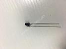
Part Number | M24C16-DRMN3TP/K |
---|---|
Manufacturer | STMicroelectronics |
Description | IC EEPROM 16KBIT 400KHZ 8SOIC |
Datasheet | M24C16-DRMN3TP/K Datasheet |
Package | 8-SOIC (0.154", 3.90mm Width) |
In Stock | 341 piece(s) |
Unit Price | $ 0.2858 * |
Lead Time | Can Ship Immediately |
Estimated Delivery Time | Jan 28 - Feb 2 (Choose Expedited Shipping) |
Request for Quotation |
|
Part Number # M24C16-DRMN3TP/K (Memory) is manufactured by STMicroelectronics and distributed by Heisener. Being one of the leading electronics distributors, we carry many kinds of electronic components from some of the world’s top class manufacturers. Their quality is guaranteed by its stringent quality control to meet all required standards.
For M24C16-DRMN3TP/K specifications/configurations, quotation, lead time, payment terms of further enquiries please have no hesitation to contact us. To process your RFQ, please add M24C16-DRMN3TP/K with quantity into BOM. Heisener.com does NOT require any registration to request a quote of M24C16-DRMN3TP/K.
Manufacturer | STMicroelectronics |
Category | Integrated Circuits (ICs) - Memory |
Datasheet | M24C16-DRMN3TP/KDatasheet |
Package | 8-SOIC (0.154", 3.90mm Width) |
Series | Automotive, AEC-Q100 |
Memory Type | Non-Volatile |
Memory Format | EEPROM |
Technology | EEPROM |
Memory Size | 16Kb (2K x 8) |
Memory Interface | I2C |
Clock Frequency | 1MHz |
Write Cycle Time - Word, Page | 4ms |
Access Time | 450ns |
Voltage - Supply | 1.7 V ~ 5.5 V |
Operating Temperature | -40°C ~ 125°C (TA) |
Mounting Type | Surface Mount |
Package / Case | 8-SOIC (0.154", 3.90mm Width) |
Supplier Device Package | 8-SO |
This is information on a product in full production. February 2016 DocID025622 Rev 6 1/38 M24C16-A125 Automotive 16-Kbit serial I²C bus EEPROM with 1 MHz clock Datasheet - production data Features • Compatible with all I2C bus modes – 1 MHz – 400 kHz – 100 kHz • Memory array – 16 Kbits (2 Kbytes) of EEPROM – Page size: 16 bytes – Additional Write lockable page (Identification page) • Extended temperature and voltage ranges – -40 °C to 125 °C; 1.7 V to 5.5 V • Schmitt trigger inputs for noise filtering • Short Write cycle time – Byte Write within 4 ms – Page Write within 4 ms • Write cycle endurance – 4 million Write cycles at 25 °C – 1.2 million Write cycles at 85 °C – 600 k Write cycles at 125 °C • Data retention – 50 years at 125 °C – 100 years at 25 °C • ESD Protection (Human Body Model) – 4000 V • Packages – RoHS compliant and halogen-free (ECOPACK2®) SO8 (MN) TSSOP8 (DW) WFDFPN8 (MF) 2 x 3 mm 169 mil width 150 mil width www.st.com
Contents M24C16-A125 2/38 DocID025622 Rev 6 Contents 1 Description . . . . . . . . . . . . . . . . . . . . . . . . . . . . . . . . . . . . . . . . . . . . . . . . . 6 2 Signal description . . . . . . . . . . . . . . . . . . . . . . . . . . . . . . . . . . . . . . . . . . . 8 2.1 Serial Clock (SCL) . . . . . . . . . . . . . . . . . . . . . . . . . . . . . . . . . . . . . . . . . . . 8 2.2 Serial Data (SDA) . . . . . . . . . . . . . . . . . . . . . . . . . . . . . . . . . . . . . . . . . . . . 8 2.3 Write Control (WC) . . . . . . . . . . . . . . . . . . . . . . . . . . . . . . . . . . . . . . . . . . . 8 2.4 VSS (ground) . . . . . . . . . . . . . . . . . . . . . . . . . . . . . . . . . . . . . . . . . . . . . . . 8 2.5 Supply voltage (VCC) . . . . . . . . . . . . . . . . . . . . . . . . . . . . . . . . . . . . . . . . . 8 3 Device operation . . . . . . . . . . . . . . . . . . . . . . . . . . . . . . . . . . . . . . . . . . . . 9 3.1 Start condition . . . . . . . . . . . . . . . . . . . . . . . . . . . . . . . . . . . . . . . . . . . . . . 10 3.2 Stop condition . . . . . . . . . . . . . . . . . . . . . . . . . . . . . . . . . . . . . . . . . . . . . . 10 3.3 Data input . . . . . . . . . . . . . . . . . . . . . . . . . . . . . . . . . . . . . . . . . . . . . . . . . 10 3.4 Acknowledge bit (ACK) . . . . . . . . . . . . . . . . . . . . . . . . . . . . . . . . . . . . . . 10 3.5 Device addressing . . . . . . . . . . . . . . . . . . . . . . . . . . . . . . . . . . . . . . . . . . .11 3.6 Identification page . . . . . . . . . . . . . . . . . . . . . . . . . . . . . . . . . . . . . . . . . . 12 4 Instructions . . . . . . . . . . . . . . . . . . . . . . . . . . . . . . . . . . . . . . . . . . . . . . . 13 4.1 Write operations . . . . . . . . . . . . . . . . . . . . . . . . . . . . . . . . . . . . . . . . . . . . 13 4.1.1 Byte Write . . . . . . . . . . . . . . . . . . . . . . . . . . . . . . . . . . . . . . . . . . . . . . . 14 4.1.2 Page Write . . . . . . . . . . . . . . . . . . . . . . . . . . . . . . . . . . . . . . . . . . . . . . . 15 4.1.3 Write Identification Page . . . . . . . . . . . . . . . . . . . . . . . . . . . . . . . . . . . . 16 4.1.4 Lock Identification Page . . . . . . . . . . . . . . . . . . . . . . . . . . . . . . . . . . . . . 16 4.1.5 Minimizing Write delays by polling on ACK . . . . . . . . . . . . . . . . . . . . . . 17 4.2 Read operations . . . . . . . . . . . . . . . . . . . . . . . . . . . . . . . . . . . . . . . . . . . . 18 4.2.1 Random Address Read . . . . . . . . . . . . . . . . . . . . . . . . . . . . . . . . . . . . . 18 4.2.2 Current Address Read . . . . . . . . . . . . . . . . . . . . . . . . . . . . . . . . . . . . . . 19 4.2.3 Sequential Read . . . . . . . . . . . . . . . . . . . . . . . . . . . . . . . . . . . . . . . . . . 19 4.2.4 Read Identification Page . . . . . . . . . . . . . . . . . . . . . . . . . . . . . . . . . . . . 19 4.2.5 Read the lock status . . . . . . . . . . . . . . . . . . . . . . . . . . . . . . . . . . . . . . . 19 4.2.6 Acknowledge in Read mode . . . . . . . . . . . . . . . . . . . . . . . . . . . . . . . . . 20 5 Application design recommendations . . . . . . . . . . . . . . . . . . . . . . . . . 21
DocID025622 Rev 6 3/38 M24C16-A125 Contents 3 5.1 Supply voltage . . . . . . . . . . . . . . . . . . . . . . . . . . . . . . . . . . . . . . . . . . . . . 21 5.1.1 Operating supply voltage (VCC) . . . . . . . . . . . . . . . . . . . . . . . . . . . . . . . 21 5.1.2 Power-up conditions . . . . . . . . . . . . . . . . . . . . . . . . . . . . . . . . . . . . . . . 21 5.1.3 Power-down . . . . . . . . . . . . . . . . . . . . . . . . . . . . . . . . . . . . . . . . . . . . . . 21 5.2 Error correction code (ECC x 1) . . . . . . . . . . . . . . . . . . . . . . . . . . . . . . . . 21 6 Delivery state . . . . . . . . . . . . . . . . . . . . . . . . . . . . . . . . . . . . . . . . . . . . . . 22 7 Maximum rating . . . . . . . . . . . . . . . . . . . . . . . . . . . . . . . . . . . . . . . . . . . . 22 8 DC and AC parameters . . . . . . . . . . . . . . . . . . . . . . . . . . . . . . . . . . . . . . 23 9 Package mechanical data . . . . . . . . . . . . . . . . . . . . . . . . . . . . . . . . . . . . 30 9.1 TSSOP8 package information . . . . . . . . . . . . . . . . . . . . . . . . . . . . . . . . . 31 9.2 SO8N package information . . . . . . . . . . . . . . . . . . . . . . . . . . . . . . . . . . . 32 9.3 WFDFPN8 package information . . . . . . . . . . . . . . . . . . . . . . . . . . . . . . . . 33 10 Part numbering . . . . . . . . . . . . . . . . . . . . . . . . . . . . . . . . . . . . . . . . . . . . 35 11 Revision history . . . . . . . . . . . . . . . . . . . . . . . . . . . . . . . . . . . . . . . . . . . 37
List of tables M24C16-A125 4/38 DocID025622 Rev 6 List of tables Table 1. Signal names . . . . . . . . . . . . . . . . . . . . . . . . . . . . . . . . . . . . . . . . . . . . . . . . . . . . . . . . . . . . 7 Table 2. Device select code . . . . . . . . . . . . . . . . . . . . . . . . . . . . . . . . . . . . . . . . . . . . . . . . . . . . . . . 11 Table 3. Significant address bits . . . . . . . . . . . . . . . . . . . . . . . . . . . . . . . . . . . . . . . . . . . . . . . . . . . . 11 Table 4. Device identification code . . . . . . . . . . . . . . . . . . . . . . . . . . . . . . . . . . . . . . . . . . . . . . . . . . 12 Table 5. Absolute maximum ratings . . . . . . . . . . . . . . . . . . . . . . . . . . . . . . . . . . . . . . . . . . . . . . . . . 22 Table 6. Operating conditions (voltage range R) . . . . . . . . . . . . . . . . . . . . . . . . . . . . . . . . . . . . . . . 23 Table 7. AC measurement conditions. . . . . . . . . . . . . . . . . . . . . . . . . . . . . . . . . . . . . . . . . . . . . . . . 23 Table 8. Input parameters. . . . . . . . . . . . . . . . . . . . . . . . . . . . . . . . . . . . . . . . . . . . . . . . . . . . . . . . . 24 Table 9. Cycling performance. . . . . . . . . . . . . . . . . . . . . . . . . . . . . . . . . . . . . . . . . . . . . . . . . . . . . . 24 Table 10. DC characteristics. . . . . . . . . . . . . . . . . . . . . . . . . . . . . . . . . . . . . . . . . . . . . . . . . . . . . . . . 25 Table 11. 400 kHz AC characteristics. . . . . . . . . . . . . . . . . . . . . . . . . . . . . . . . . . . . . . . . . . . . . . . . . 26 Table 12. 1 MHz AC characteristics . . . . . . . . . . . . . . . . . . . . . . . . . . . . . . . . . . . . . . . . . . . . . . . . . . 27 Table 13. TSSOP8 – 3x4.4 mm, 0.65 mm pitch, 8-lead thin shrink small outline, package mechanical data . . . . . . . . . . . . . . . . . . . . . . . . . . . . . . . . . . . . . . . . . . . . . . . . . . 31 Table 14. SO8N – 3.9x4.9 mm, 8-lead plastic small outline, 150 mils body width, package mechanical data . . . . . . . . . . . . . . . . . . . . . . . . . . . . . . . . . . . . . . . . . . . . . . . . . . 32 Table 15. WFDFPN8 (MLP8) – 8-lead, 2 x 3 mm, 0.5 mm pitch very thin fine pitch dual flat package mechanical data . . . . . . . . . . . . . . . . . . . . . . . . . . . . . . . . . . . . . . . . . . . 34 Table 16. Ordering information scheme . . . . . . . . . . . . . . . . . . . . . . . . . . . . . . . . . . . . . . . . . . . . . . . 35 Table 17. Document revision history . . . . . . . . . . . . . . . . . . . . . . . . . . . . . . . . . . . . . . . . . . . . . . . . . 37
DocID025622 Rev 6 5/38 M24C16-A125 List of figures 5 List of figures Figure 1. Logic diagram . . . . . . . . . . . . . . . . . . . . . . . . . . . . . . . . . . . . . . . . . . . . . . . . . . . . . . . . . . . . 6 Figure 2. 8-pin package connections . . . . . . . . . . . . . . . . . . . . . . . . . . . . . . . . . . . . . . . . . . . . . . . . . . 7 Figure 3. I2C bus protocol . . . . . . . . . . . . . . . . . . . . . . . . . . . . . . . . . . . . . . . . . . . . . . . . . . . . . . . . . . 9 Figure 4. Write mode sequences with WC = 0 (data write enabled) . . . . . . . . . . . . . . . . . . . . . . . . . 14 Figure 5. Write mode sequences with WC = 1 (data write inhibited) . . . . . . . . . . . . . . . . . . . . . . . . . 15 Figure 6. Write cycle polling flowchart using ACK . . . . . . . . . . . . . . . . . . . . . . . . . . . . . . . . . . . . . . . 17 Figure 7. Read mode sequences. . . . . . . . . . . . . . . . . . . . . . . . . . . . . . . . . . . . . . . . . . . . . . . . . . . . 18 Figure 8. AC measurement I/O waveform . . . . . . . . . . . . . . . . . . . . . . . . . . . . . . . . . . . . . . . . . . . . . 23 Figure 9. Maximum Rbus value versus bus parasitic capacitance (Cbus) for an I 2C bus at maximum frequency fC = 400 kHz . . . . . . . . . . . . . . . . . . . . . . . . . . . . . . . . . . . . . 28 Figure 10. Maximum Rbus value versus bus parasitic capacitance Cbus) for an I 2C bus at maximum frequency fC = 1MHz . . . . . . . . . . . . . . . . . . . . . . . . . . . . . . . . . . . . . . . 28 Figure 11. AC waveforms . . . . . . . . . . . . . . . . . . . . . . . . . . . . . . . . . . . . . . . . . . . . . . . . . . . . . . . . . . 29 Figure 12. TSSOP8 – 3x4.4 mm, 0.65 mm pitch, 8-lead thin shrink small outline, package outline. . . . . . . . . . . . . . . . . . . . . . . . . . . . . . . . . . . . . . . . . . . . . . . . . . . . . . . . . . 31 Figure 13. SO8N – 3.9x4.9 mm, 8-lead plastic small outline, 150 mils body width, package outline. . . . . . . . . . . . . . . . . . . . . . . . . . . . . . . . . . . . . . . . . . . . . . . . . . . . . . . . . . 32 Figure 14. WFDFPN8 (MLP8) – 8-lead, 2 x 3 mm, 0.5 mm pitch very very thin fine pitch dual flat package outline . . . . . . . . . . . . . . . . . . . . . . . . . . . . . . . . . . . . . . . . . . . . . . . . . . . 33
Description M24C16-A125 6/38 DocID025622 Rev 6 1 Description The M24C16-A125 is a 16-Kbit serial EEPROM Automotive grade device operating up to 125 °C. The M24C16-A125 is compliant with the very high level of reliability defined by the Automotive standard AEC-Q100 grade 1. The device is accessed by a simple serial I2C compatible interface running up to 1 MHz. The memory array is based on advanced true EEPROM technology (electrically erasable programmable memory). The M24C16-A125 is a byte-alterable memory (2048 × 8 bits) organized as 128 pages of 16 bytes in which the data integrity is significantly improved with an embedded Error Correction Code logic. The M24C16-A125 offers an additional Identification Page (16 bytes) in which the ST device identification can be read. This page can also be used to store sensitive application parameters which can be later permanently locked in read-only mode. Figure 1. Logic diagram
DocID025622 Rev 6 7/38 M24C16-A125 Description 37 Figure 2. 8-pin package connections 1. See Section 9: Package mechanical data for package dimensions, and how to identify pin 1. Table 1. Signal names Signal name Function Direction SDA Serial Data I/O SCL Serial Clock Input WC Write Control Input VCC Supply voltage - VSS Ground -
Signal description M24C16-A125 8/38 DocID025622 Rev 6 2 Signal description 2.1 Serial Clock (SCL) The signal applied on this input is used to strobe the data available on SDA(in) and to output the data on SDA(out). 2.2 Serial Data (SDA) SDA is an input/output used to transfer data in or out of the device. SDA(out) is an open drain output that may be wire-OR’ed with other open drain or open collector signals on the bus. A pull up resistor must be connected between SDA and VCC (Figure 9 and Figure 10 indicate how to calculate the value of the pull-up resistor). 2.3 Write Control (WC) This input signal is useful for protecting the entire contents of the memory from inadvertent write operations. Write operations are disabled to the entire memory array when Write Control (WC) is driven high. Write operations are enabled when Write Control (WC) is either driven low or left floating. When Write Control (WC) is driven high, device select and address bytes are acknowledged, Data bytes are not acknowledged. 2.4 VSS (ground) VSS is the reference for the VCC supply voltage. 2.5 Supply voltage (VCC) VCC is the supply voltage pin.
DocID025622 Rev 6 9/38 M24C16-A125 Device operation 37 3 Device operation The device supports the I2C protocol (see Figure 3). The I2C bus is controlled by the bus master and the device is always a slave in all communications. The device (bus master or a slave) that sends data on to the bus is defined as a transmitter; the device (bus master or a slave) is defined as a receiver when reading the data. Figure 3. I2C bus protocol
Kel***** Jain
December 24, 2020
Darr*****ugar
December 21, 2020
Palo*****rimes
December 19, 2020
Jayson*****nathan
December 3, 2020
Rhe*****hmed
December 1, 2020
Russ*****Lucero
November 25, 2020
Aval*****Bhasin
November 22, 2020
Itza***** Liu
November 16, 2020
We guarantee 100% customer satisfaction.
Our experienced sales team and tech support team back our services to satisfy all our customers.
We provide 90 days warranty.
If the items you received were not in perfect quality, we would be responsible for your refund or replacement, but the items must be returned in their original condition.
Payment Methods | |
Delivery Services |
Heisener's commitment to quality has shaped our processes for sourcing, testing, shipping, and every step in between. This foundation underlies each component we sell.