Part Number | MAX1090ACEI+ |
---|---|
Manufacturer | Maxim Integrated |
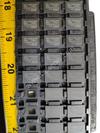
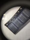
Description | IC ADC 10BIT 400KSPS 28-QSOP |
Datasheet | MAX1090ACEI+ Datasheet |
Package | 28-SSOP (0.154", 3.90mm Width) |
In Stock | 2,000 piece(s) |
Unit Price | $ 9.0000 * |
Lead Time | Can Ship Immediately |
Estimated Delivery Time | Jan 28 - Feb 2 (Choose Expedited Shipping) |
Request for Quotation |
|
Part Number # MAX1090ACEI+ (Data Acquisition - Analog to Digital Converters (ADC)) is manufactured by Maxim Integrated and distributed by Heisener. Being one of the leading electronics distributors, we carry many kinds of electronic components from some of the world’s top class manufacturers. Their quality is guaranteed by its stringent quality control to meet all required standards.
For MAX1090ACEI+ specifications/configurations, quotation, lead time, payment terms of further enquiries please have no hesitation to contact us. To process your RFQ, please add MAX1090ACEI+ with quantity into BOM. Heisener.com does NOT require any registration to request a quote of MAX1090ACEI+.
Manufacturer | Maxim Integrated |
Category | Integrated Circuits (ICs) - Data Acquisition - Analog to Digital Converters (ADC) |
Datasheet | MAX1090ACEI+Datasheet |
Package | 28-SSOP (0.154", 3.90mm Width) |
Series | - |
Number of Bits | 10 |
Sampling Rate (Per Second) | 400k |
Number of Inputs | 4, 8 |
Input Type | Pseudo-Differential, Single Ended |
Data Interface | Parallel |
Configuration | MUX-S/H-ADC |
Ratio - S/H:ADC | 1:1 |
Number of A/D Converters | 1 |
Architecture | SAR |
Reference Type | External, Internal |
Voltage - Supply, Analog | 5V |
Voltage - Supply, Digital | 2.7 V ~ 5.5 V |
Features | - |
Operating Temperature | 0°C ~ 70°C |
Package / Case | 28-SSOP (0.154", 3.90mm Width) |
Supplier Device Package | 28-QSOP |
Mounting Type | - |
For pricing, delivery, and ordering information, please contact Maxim/Dallas Direct! at 1-888-629-4642, or visit Maxim’s website at www.maxim-ic.com. General Description The MAX1090/MAX1092 low-power, 10-bit analog-to- digital converters (ADCs) feature a successive-approxi- mation ADC, automatic power-down, fast wake-up (2µs), an on-chip clock, +2.5V internal reference, and a high-speed, byte-wide parallel interface. The devices operate with a single +5V analog supply and feature a VLOGIC pin that allows them to interface directly with a +2.7V to +5.5V digital supply. Power consumption is only 10mW (VDD = VLOGIC) at a 400ksps max sampling rate. Two software-selectable power-down modes enable the MAX1090/MAX1092 to be shut down between conversions; accessing the par- allel interface returns them to normal operation. Powering down between conversions can cut supply current to under 10µA at reduced sampling rates. Both devices offer software-configurable analog inputs for unipolar/bipolar and single-ended/pseudo-differen- tial operation. In single-ended mode, the MAX1090 has eight input channels and the MAX1092 has four input channels (four and two input channels, respectively, when in pseudo-differential mode). Excellent dynamic performance and low power, com- bined with ease of use and small package size, make these converters ideal for battery-powered and data- acquisition applications or for other circuits with demand- ing power consumption and space requirements. The MAX1090/MAX1092 tri-states INT when CS goes high. Refer to the MAX1060/MAX1064 if tri-stating INT is not desired. The MAX1090 is available in a 28-pin QSOP package, while the MAX1092 comes in a 24-pin QSOP. For pin- compatible +3V, 10-bit versions, refer to the MAX1091/ MAX1093 data sheet. Applications Industrial Control Systems Data Logging Energy Management Patient Monitoring Data-Acquisition Systems Touchscreens Features 10-Bit Resolution, ±0.5 LSB Linearity +5V Single-Supply Operation User-Adjustable Logic Level (+2.7V to +5.5V) Internal +2.5V Reference Software-Configurable Analog Input Multiplexer 8-Channel Single-Ended/ 4-Channel Pseudo-Differential (MAX1090) 4-Channel Single-Ended/ 2-Channel Pseudo-Differential (MAX1092) Software-Configurable Unipolar/Bipolar Analog Inputs Low Current: 2.5mA (400ksps) 1.0mA (100ksps) 400µA (10ksps) 2µA (Shutdown) Internal 6MHz Full-Power Bandwidth Track/Hold Byte-Wide Parallel (8 + 2) Interface Small Footprint: 28-Pin QSOP (MAX1090) 24-Pin QSOP (MAX1092) M A X 1 0 9 0 /M A X 1 0 9 2 400ksps, +5V, 8-/4-Channel, 10-Bit ADCs with +2.5V Reference and Parallel Interface ________________________________________________________________ Maxim Integrated Products 1 19-1640; Rev 2; 12/02 PART MAX1090ACEI 0°C to +70°C TEMP RANGE PIN-PACKAGE 28 QSOP Ordering Information Pin Configurations ±0.5 INL (LSB) MAX1090BCEI 0°C to +70°C ±128 QSOP MAX1090BEEI MAX1090AEEI -40°C to +85°C ±1 -40°C to +85°C ±0.528 QSOP 28 QSOP Ordering Information continued at end of data sheet. Typical Operating Circuits appear at end of data sheet. 24 23 22 21 20 19 18 17 16 15 14 13 1 2 3 4 5 6 7 8 9 10 11 12 VLOGIC VDD REF REFADJ GND COM CH0 CH1 CH2 CH3 CS CLKWR RD INT D0/D8 D1/D9 D2 D3 D4 D5 D6 D7 HBEN QSOP MAX1092 TOP VIEW Pin Configurations continued at end of data sheet. EVALU ATION KIT AVAIL ABLE
M A X 1 0 9 0 /M A X 1 0 9 2 400ksps, +5V, 8-/4-Channel, 10-Bit ADCs with +2.5V Reference and Parallel Interface 2 _______________________________________________________________________________________ ABSOLUTE MAXIMUM RATINGS ELECTRICAL CHARACTERISTICS (VDD = VLOGIC = +5V ±10%, COM = GND, REFADJ = VDD, VREF = +2.5V, 4.7µF capacitor at REF pin, fCLK = 7.6MHz (50% duty cycle), TA = TMIN to TMAX, unless otherwise noted. Typical values are at TA = +25°C.) Stresses beyond those listed under “Absolute Maximum Ratings” may cause permanent damage to the device. These are stress ratings only, and functional operation of the device at these or any other conditions beyond those indicated in the operational sections of the specifications is not implied. Exposure to absolute maximum rating conditions for extended periods may affect device reliability. External acquisition or external clock mode Internal acquisition/internal clock mode MAX109_A External acquisition/internal clock mode External clock mode -3dB rolloff SINAD > 56dB fIN = 175kHz, VIN = 2.5VP-P (Note 4) fIN1 = 49kHz, fIN2 = 52kHz MAX109_B No missing codes over temperature CONDITIONS ns25Aperture Delay ns400tACQT/H Acquisition Time µs 3.2 3.6 4 2.5 3.0 3.5 2.1 tCONVConversion Time (Note 5) MHz6Full-Power Bandwidth kHz350Full-Linear Bandwidth dB-78Channel-to-Channel Crosstalk dB76IMDIntermodulation Distortion dB72SFDRSpurious-Free Dynamic Range dB-72 Total Harmonic Distortion (including 5th-order harmonic) THD ±0.5 INLRelative Accuracy (Note 2) Bits10RESResolution dB60SINADSignal-to-Noise Plus Distortion LSB±0.1 Channel-to-Channel Offset Matching ppm/°C±2.0Gain Temperature Coefficient LSB ±1 LSB±1DNLDifferential Nonlinearity LSB±2Offset Error LSB±2Gain Error (Note 3) UNITSMIN TYP MAXSYMBOLPARAMETER Internal acquisition/internal clock mode External acquisition or external clock mode <200 ps <50 Aperture Jitter MHz0.1 7.6fCLKExternal Clock Frequency %30 70Duty Cycle DC ACCURACY (Note 1) DYNAMIC SPECIFICATIONS (fIN(sine wave) = 50kHz, VIN = 2.5VP-P, 400ksps, external fCLK = 7.6MHz, bipolar input mode) CONVERSION RATE VDD to GND..............................................................-0.3V to +6V VLOGIC to GND.........................................................-0.3V to +6V CH0–CH7, COM to GND............................-0.3V to (VDD + 0.3V) REF, REFADJ to GND.................................-0.3V to (VDD + 0.3V) Digital Inputs to GND ...............................................-0.3V to +6V Digital Outputs (D0–D9, INT) to GND ........................................... -0.3V to (VLOGIC + 0.3V) Continuous Power Dissipation (TA = +70°C) 24-Pin QSOP (derate 9.5mW/°C above +70°C).........762mW 28-Pin QSOP (derate 8.00mW/°C above +70°C).......667mW Operating Temperature Ranges MAX1090_C_ _/MAX1092_C_ _....................... 0°C to +70°C MAX1090_E_ _/MAX1092_E_ _ .....................-40°C to +85°C Storage Temperature Range .............................-65°C to +150°C Lead Temperature (soldering, 10s) .................................+300°C
V M A X 1 0 9 0 /M A X 1 0 9 2 400ksps, +5V, 8-/4-Channel, 10-Bit ADCs with +2.5V Reference and Parallel Interface _______________________________________________________________________________________ 3 ELECTRICAL CHARACTERISTICS (continued) (VDD = VLOGIC = +5V ±10%, COM = GND, REFADJ = VDD, VREF = +2.5V, 4.7µF capacitor at REF pin, fCLK = 7.6MHz (50% duty cycle), TA = TMIN to TMAX, unless otherwise noted. Typical values are at TA = +25°C.) CONDITIONS UNITSMIN TYP MAXSYMBOLPARAMETER 0 to 0.5mA output load To power down the internal reference For small adjustments On/off-leakage current, VIN = 0 or VDD Unipolar, VCOM = 0 V1.0 VDD + 50mV VREFREF Input Voltage Range µF4.7 10Capacitive Bypass at REF µF0.01 1Capacitive Bypass at REFADJ mV/mA0.2Load Regulation (Note 7) VVDD - 1.0REFADJ High Threshold mV±100REFADJ Input Range ±20 ppm/°CTCREFREF Temperature Coefficient mA15REF Short-Circuit Current V2.49 2.5 2.51REF Output Voltage pF12CINInput Capacitance µA±0.01 ±1Multiplexer Leakage Current V Analog Input Voltage Range, Single Ended and Differential (Note 6) 0 VREF VIN CS = VDD ISOURCE = 1mA ISINK = 1.6mA VIN = 0 or VDD VLOGIC = 4.5V or 2.7V VLOGIC = 4.5V µA±0.1 ±1ILEAKAGEThree-State Leakage Current VVLOGIC - 0.5VOHOutput Voltage High V0.4VOLOutput Voltage Low pF15CINInput Capacitance µA±0.1 ±1IINInput Leakage Current mV200VHYSInput Hysteresis V0.8VILInput Voltage Low V 4.0 CS = VDD pF15COUTThree-State Output Capacitance Bipolar, VCOM = VREF / 2 -VREF/2 +VREF/2 VLOGIC = 2.7V 2.0 VIHInput Voltage High TA = 0°C to +70°C VREF = 2.5V, fSAMPLE = 400ksps 200 300 Shutdown mode µA 2 IREFShutdown REF Input Current ANALOG INPUTS INTERNAL REFERENCE EXTERNAL REFERENCE AT REF DIGITAL INPUTS AND OUTPUTS
Operating mode, M A X 1 0 9 0 /M A X 1 0 9 2 400ksps, +5V, 8-/4-Channel, 10-Bit ADCs with +2.5V Reference and Parallel Interface 4 _______________________________________________________________________________________ TIMING CHARACTERISTICS (VDD = VLOGIC = +5V ±10%, COM = GND, REFADJ = VDD, VREF = +2.5V, 4.7µF capacitor at REF pin, fCLK = 7.6MHz (50% duty cycle), TA = TMIN to TMAX, unless otherwise noted. Typical values are at TA = +25°C.) CONDITIONS UNITSMIN TYP MAXSYMBOLPARAMETER Standby mode Operating mode, fSAMPLE = 400ksps 1.0 1.2 mA 2.5 2.9 2.9 3.4 IDDPositive Supply Current V4.5 5.5VDDAnalog Supply Voltage 200 ELECTRICAL CHARACTERISTICS (continued) (VDD = VLOGIC = +5V ±10%, COM = GND, REFADJ = VDD, VREF = +2.5V, 4.7µF capacitor at REF pin, fCLK = 7.6MHz (50% duty cycle), TA = TMIN to TMAX, unless otherwise noted. Typical values are at TA = +25°C.) VLOGIC Current ILOGIC CL = 20pF 2 10 µA Power-Supply Rejection PSR VDD = 5V ±10%, full-scale input ±0.3 ±0.9 mV fSAMPLE = 400ksps Nonconverting V2.7 VDD + 0.3 VLOGICDigital Supply Voltage WR to CLK Fall Setup Time tCWS 40 ns nsCLK Pulse Width High nsCLK Period tCH 40 tCP 132 CLK Pulse Width Low tCL 40 ns Data Valid to WR Rise Time tDS 40 ns WR Rise to Data Valid Hold Time tDH 0 ns CLK Fall to WR Hold Time tCWH 40 ns CS to CLK or WR Setup Time tCSWS 60 ns CLK or WR to CS Hold Time tCSWH 0 ns CS Pulse Width tCS 100 ns WR Pulse Width (Note 8) tWR 60 ns PARAMETER SYMBOL MIN TYP MAX UNITSCONDITIONS Shutdown mode 2 10 0.5 0.8 POWER REQUIREMENTS µA External reference Internal reference External reference Internal reference
M A X 1 0 9 0 /M A X 1 0 9 2 400ksps, +5V, 8-/4-Channel, 10-Bit ADCs with +2.5V Reference and Parallel Interface _______________________________________________________________________________________ 5 Note 1: Tested at VDD = +5V, COM = GND, unipolar single-ended input mode. Note 2: Relative accuracy is the deviation of the analog value at any code from its theoretical value after offset and gain errors have been removed. Note 3: Offset nulled. Note 4: On channel is grounded; sine wave applied to off channels. Note 5: Conversion time is defined as the number of clock cycles times the clock period; clock has 50% duty cycle. Note 6: Input voltage range referenced to negative input. The absolute range for the analog inputs is from GND to VDD. Note 7: External load should not change during conversion for specified accuracy. Note 8: When bit 5 is set low for internal acquisition, WR must not return low until after the first falling clock edge of the conversion. TIMING CHARACTERISTICS (continued) (VDD = VLOGIC = +5V ±10%, COM = GND, REFADJ = VDD, VREF = +2.5V, 4.7µF capacitor at REF pin, fCLK = 7.6MHz (50% duty cycle), TA = TMIN to TMAX, unless otherwise noted. Typical values are at TA = +25°C.) 3kΩ 3kΩ DOUT DOUT VLOGIC a) HIGH-Z TO VOH AND VOL TO VOH b) HIGH-Z TO VOL AND VOH TO VOL CLOAD 20pF CLOAD 20pF Figure 1. Load Circuits for Enable/Disable Times tTR 10 40 nsCLOAD = 20pF, Figure 1RD Rise to Output Disable RD Fall to Output Data Valid tDO 10 50 ns RD Fall to INT High Delay tINT1 50 ns CS Fall to Output Data Valid tDO2 100 ns CLOAD = 20pF, Figure 1 CLOAD = 20pF, Figure 1 CLOAD = 20pF, Figure 1 tTC 10 60 nsCLOAD = 20pF, Figure 1 PARAMETER SYMBOL MIN TYP MAX UNITSCONDITIONS CS Rise to Output Disable HBEN Rise to Output Data Valid tDO1 10 50 nsCLOAD = 20pF, Figure 1 HBEN Fall to Output Data Valid tDO1 10 80 nsCLOAD = 20pF, Figure 1
M A X 1 0 9 0 /M A X 1 0 9 2 400ksps, +5V, 8-/4-Channel, 10-Bit ADCs with +2.5V Reference and Parallel Interface 6 _______________________________________________________________________________________ Typical Operating Characteristics (VDD = VLOGIC = +5V, VREF = +2.500V, fCLK = 7.6MHz, CL = 20pF, TA = +25°C, unless otherwise noted.) -0.25 -0.10 -0.15 -0.20 -0.05 0 0.05 0.10 0.15 0.20 0.25 0 400200 600 800 1000 1200 INTEGRAL NONLINEARITY vs. OUTPUT CODE M A X 1 0 9 0 /9 2 t o c0 1 OUTPUT CODE IN L (L S B ) 0.1 10k101 100 1k 100k 1M SUPPLY CURRENT vs. SAMPLE FREQUENCY M A X 1 0 9 0 /9 2 t o c0 3 fSAMPLE (Hz) I D D ( µA ) 1 10 100 1k 10k WITH INTERNAL REFERENCE WITH EXTERNAL REFERENCE 1.8 1.9 2.0 2.1 2.2 SUPPLY CURRENT vs. SUPPLY VOLTAGE M A X 1 0 9 0 /9 2 t o c0 4 VDD (V) I D D ( m A ) 4.50 5.004.75 5.25 5.50 RL = ∞ CODE = 1010100000 1.7 1.9 1.8 2.1 2.0 2.2 2.3 -40 10-15 35 60 85 SUPPLY CURRENT vs. TEMPERATURE M A X 1 0 9 0 /9 2 t o c0 5 TEMPERATURE (°C) I D D ( m A ) RL = ∞ CODE = 1010100000 930 950 940 970 960 980 990 4.50 5.004.75 5.25 5.50 STANDBY CURRENT vs. SUPPLY VOLTAGE M A X 1 0 9 0 /9 2 t o c0 6 VDD (V) S TA N D B Y I D D ( µA ) 930 950 940 970 960 980 990 -40 10-15 35 60 85 STANDBY CURRENT vs. TEMPERATURE M A X 1 0 9 0 /9 2 t o c0 7 TEMPERATURE (°C) S TA N D B Y I D D ( µA ) 1.0 1.5 2.0 2.5 3.0 POWER-DOWN CURRENT vs. SUPPLY VOLTAGE M A X 1 0 9 0 /9 2 t o c0 8 VDD (V) P O W ER -D O W N I D D ( µA ) 4.50 5.004.75 5.25 5.50 1.8 2.0 1.9 2.1 2.2 -40 10-15 35 60 85 POWER-DOWN CURRENT vs. TEMPERATURE M A X 1 0 9 0 /9 2 t o c0 9 TEMPERATURE (°C) P O W ER -D O W N I D D ( µA ) -0.25 -0.10 -0.15 -0.20 -0.05 0 0.05 0.10 0.15 0.20 0.25 0 400200 600 800 1000 1200 DIFFERENTIAL NONLINEARITY vs. OUTPUT CODE M A X 1 0 9 0 /9 2 t o c0 2 OUTPUT CODE D N L (L S B )
M A X 1 0 9 0 /M A X 1 0 9 2 400ksps, +5V, 8-/4-Channel, 10-Bit ADCs with +2.5V Reference and Parallel Interface _______________________________________________________________________________________ 7 2.48 2.49 2.51 2.50 2.52 2.53 INTERNAL REFERENCE VOLTAGE vs. SUPPLY VOLTAGE M A X 1 0 9 0 /9 2 t o c1 0 VDD (V) V R EF ( V ) 4.50 5.004.75 5.25 5.50 2.48 2.49 2.51 2.50 2.52 2.53 -40 10-15 35 60 85 INTERNAL REFERENCE VOLTAGE vs. TEMPERATURE M A X 1 0 9 0 /9 2 t o c 1 1 TEMPERATURE (°C) V R EF ( V ) 1.0 0.5 0 -0.5 -1.0 4.50 5.004.75 5.25 5.50 OFFSET ERROR vs. SUPPLY VOLTAGE M A X 1 0 9 0 /9 2 t o c1 2 VDD (V) O FF S ET E R R O R ( LS B ) 1.0 0.5 0 -0.5 -1.0 -40 10-15 35 60 85 OFFSET ERROR vs. TEMPERATURE M A X 1 0 9 0 /9 2 t o c1 3 TEMPERATURE (°C) O FF S ET E R R O R ( LS B ) -0.50 0 -0.25 0.25 0.50 GAIN ERROR vs. SUPPLY VOLTAGE M A X 1 0 9 0 /9 2 t o c1 4 VDD (V) G A IN E R R O R ( LS B ) 4.50 5.004.75 5.25 5.50 0 0.125 0.250 0.375 0.500 GAIN ERROR vs. TEMPERATURE M A X 1 0 9 0 /9 2 t o c1 5 TEMPERATURE (°C) G A IN E R R O R ( LS B ) -40 35 60-15 10 85 50 150 100 200 250 LOGIC SUPPLY CURRENT vs. SUPPLY VOLTAGE M A X 1 0 9 0 /9 2 t o c1 6 VDD (V) I L O G IC ( µA ) 4.50 5.004.75 5.25 5.50 Typical Operating Characteristics (continued) (VDD = VLOGIC = +5V, VREF = +2.500V, fCLK = 7.6MHz, CL = 20pF, TA = +25°C, unless otherwise noted.) 0 50 150 100 200 250 -40 10-15 35 60 85 LOGIC SUPPLY CURRENT vs. TEMPERATURE M A X 1 0 9 0 /9 2 t o c 1 7 TEMPERATURE (°C) I L O G IC ( µA ) -140 -120 -100 -80 -60 -40 -20 0 20 0 400200 600 800 1000 1200 FFT PLOT M A X 1 0 9 0 /9 2 t o c1 8 FREQUENCY (kHz) A M P LI TU D E (d B ) VDD = 5V fIN = 50kHz fSAMPLE = 400ksps
M A X 1 0 9 0 /M A X 1 0 9 2 400ksps, +5V, 8-/4-Channel, 10-Bit ADCs with +2.5V Reference and Parallel Interface 8 _______________________________________________________________________________________ Pin Description NAME FUNCTION 1 HBEN High Byte Enable. Used to multiplex the 10-bit conversion result. 1: 2 MSBs are multiplexed on the data bus. 0: 8 LSBs are available on the data bus. PIN 2 D7 Three-State Digital I/O Line (D7) 3 D6 Three-State Digital I/O Line (D6) 4 D5 Three-State Digital I/O Line (D5) 5 D4 Three-State Digital I/O Line (D4) 6 D3 Three-State Digital I/O Line (D3) 7 D2 Three-State Digital I/O Line (D2) 8 D1/D9 Three-State Digital I/O Line (D1, HBEN = 0; D9, HBEN = 1) 9 D0/D8 Three-State Digital I/O Line (D0, HBEN = 0; D8, HBEN = 1) 10 INT INT goes low when the conversion is complete and the output data is ready. 11 RD Active-Low Read Select. If CS is low, a falling edge on RD enables the read operation on the data bus. 12 WR Active-Low Write Select. When CS is low in internal acquisition mode, a rising edge on WR latches in configuration data and starts an acquisition plus a conversion cycle. When CS is low in external acquisition mode, the first rising edge on WR ends acquisition and starts a conversion. 13 CLK Clock Input. In external clock mode, drive CLK with a TTL/CMOS-compatible clock. In internal clock mode, connect this pin to either VDD or GND. 14 CS Active-Low Chip Select. When CS is high, digital outputs (INT, D7–D0) are high impedance. 15 CH7 Analog Input Channel 7 16 CH6 Analog Input Channel 6 17 CH5 Analog Input Channel 5 18 CH4 Analog Input Channel 4 19 CH3 Analog Input Channel 3 20 CH2 Analog Input Channel 2 21 CH1 Analog Input Channel 1 22 CH0 Analog Input Channel 0 23 COM Ground Reference for Analog Inputs. Sets zero-code voltage in single-ended mode and must be stable to ±0.5 LSB during conversion. 24 GND Analog and Digital Ground 25 REFADJ Bandgap Reference Output/Bandgap Reference Buffer Input. Bypass to GND with a 0.01µF capacitor. When using an external reference, connect REFADJ to VDD to disable the internal bandgap reference. 26 REF Bandgap Reference Buffer Output/External Reference Input. Add a 4.7µF capacitor to GND when using the internal reference. 27 VDD Analog +5V Power Supply. Bypass with a 0.1µF capacitor to GND. 28 VLOGIC Digital Power Supply. VLOGIC powers the digital outputs of the data converter and can range from +2.7V to VDD + 300mV. 1 2 3 4 5 6 7 8 9 10 11 12 13 14 — — — — 15 16 17 18 19 20 21 22 23 24 MAX1090 MAX1092
M A X 1 0 9 0 /M A X 1 0 9 2 400ksps, +5V, 8-/4-Channel, 10-Bit ADCs with +2.5V Reference and Parallel Interface _______________________________________________________________________________________ 9 Detailed Description Converter Operation The MAX1090/MAX1092 ADCs use a successive- approximation (SAR) conversion technique and an input track-and-hold (T/H) stage to convert an analog input signal to a 10-bit digital output. Their parallel (8 + 2) out- put format provides an easy interface to standard micro- processors (µPs). Figure 2 shows the simplified internal architecture of the MAX1090/MAX1092. Single-Ended and Pseudo-Differential Operation The sampling architecture of the ADC’s analog com- parator is illustrated in the equivalent input circuits in Figures 3a and 3b. In single-ended mode, IN+ is inter- nally switched to channels CH0–CH7 for the MAX1090 (Figure 3a) and to CH0–CH3 for the MAX1092 (Figure 3b), while IN- is switched to COM (Table 3). In differen- tial mode, IN+ and IN- are selected from analog input pairs (Table 4). In differential mode, IN- and IN+ are internally switched to either of the analog inputs. This configuration is pseudo- differential in that only the signal at IN+ is sampled. The return side (IN-) must remain stable within ±0.5 LSB (±0.1 LSB for best performance) with respect to GND during a conversion. To accomplish this, connect a 0.1µF capacitor from IN- (the selected input) to GND. During the acquisition interval, the channel selected as the positive input (IN+) charges capacitor CHOLD. At the end of the acquisition interval, the T/H switch opens, retaining the charge on CHOLD as a sample of the signal at IN+. The conversion interval begins with the input multiplex- er switching CHOLD from the positive input (IN+) to the negative input (IN-). This unbalances node ZERO at the comparator’s positive input. The capacitive digital-to- analog converter (DAC) adjusts during the remainder of the conversion cycle to restore node ZERO to 0V within the limits of 10-bit resolution. This action is equivalent to transferring a 12pF [(VIN+) - (VIN-)] charge from CHOLD to the binary-weighted capacitive DAC, which in turn forms a digital representation of the analog input signal. T/H THREE-STATE, BIDIRECTIONAL I/O INTERFACE 10 17kΩ 8 8 2 8 2 8 SUCCESSIVE- APPROXIMATION REGISTER MUX ( ) ARE FOR MAX1090 ONLY. CHARGE REDISTRIBUTION 10-BIT DAC CLOCK ANALOG INPUT MULTIPLEXER CONTROL LOGIC AND LATCHES REF REFADJ 1.22V REFERENCE D0–D7 8-BIT DATA BUS (CH5) (CH4) CH3 CH2 CH1 CH0 COM CLK CS WR RD INT VDD HBEN GND VLOGIC MAX1090 MAX1092 AV = 2.05 COMP (CH7) (CH6) Figure 2. Simplified Functional Diagram of 8-/4-Channel MAX1090/MAX1092
Celi*****eorge
December 21, 2020
Bel*****Sarma
December 16, 2020
Lenno*****ughese
December 14, 2020
Elai*****oods
December 12, 2020
Marce*****averi
December 10, 2020
Emmi*****odhi
December 6, 2020
We guarantee 100% customer satisfaction.
Our experienced sales team and tech support team back our services to satisfy all our customers.
We provide 90 days warranty.
If the items you received were not in perfect quality, we would be responsible for your refund or replacement, but the items must be returned in their original condition.
Payment Methods | |
Delivery Services |
Heisener's commitment to quality has shaped our processes for sourcing, testing, shipping, and every step in between. This foundation underlies each component we sell.