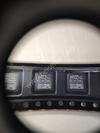
| Part Number | MAX3209EEUU |
|---|---|
| Manufacturer | Maxim Integrated |
| Description | IC TXRX LP DUAL RS232 38-TSSOP |
| Datasheet | |
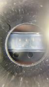
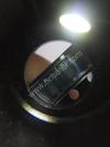
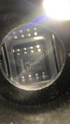
| Package | 38-TFSOP (0.173", 4.40mm Width) |
| ECAD |
|
| In Stock | 9,924 piece(s) |
| Unit Price | Request a Quote |
| Lead Time | Can Ship Immediately |
| Estimated Delivery Time | Apr 20 - Apr 25 (Choose Expedited Shipping) |
| Request for Quotation |
|
| Payment Methods | |
| Delivery Services |
Part Number # MAX3209EEUU (Interface - Drivers, Receivers, Transceivers) is manufactured by Maxim Integrated and distributed by Heisener. Being one of the leading electronics distributors, we carry many kinds of electronic components from some of the world’s top class manufacturers. Their quality is guaranteed by its stringent quality control to meet all required standards.
For MAX3209EEUU specifications/configurations, quotation, lead time, payment terms of further enquiries please have no hesitation to contact us. To process your RFQ, please add MAX3209EEUU with quantity into BOM. Heisener.com does NOT require any registration to request a quote of MAX3209EEUU.
| Manufacturer | Maxim Integrated |
| Category | Integrated Circuits (ICs) - Interface - Drivers, Receivers, Transceivers |
| Package | 38-TFSOP (0.173", 4.40mm Width) |
| ECAD |
|
| Series | - |
| Type | Transceiver |
| Protocol | RS232 |
| Number of Drivers/Receivers | 6/10 |
| Duplex | Full |
| Receiver Hysteresis | 200mV |
| Data Rate | 460Kbps |
| Voltage - Supply | 10.8 V ~ 13.2 V |
| Operating Temperature | 0°C ~ 70°C |
| Mounting Type | Surface Mount |
| Package / Case | 38-TFSOP (0.173", 4.40mm Width) |
| Supplier Device Package | 38-TSSOP |
Beat***** Shaw
April 2, 2023
Denv*****arajas
March 31, 2023
Isai*****olan
March 25, 2023
Zand*****rince
March 22, 2023
Kie*****Sha
March 17, 2023
Cols*****ecker
March 11, 2023
Calvi*****agopal
February 26, 2023
Brie*****Krish
February 23, 2023


|
ABM10AIG-20.000MHZ-4-T3 | Abracon LLC, CRYSTAL 20MHZ 10PF SMD, 4-SMD, No Lead, - | View |

|
2220J2K50471JCR | Knowles Syfer, CAP CER 2220, 2220 (5750 Metric), - | View |

|
1206J0253P30DCT | Knowles Syfer, CAP CER 1206, 1206 (3216 Metric), - | View |

|
GJM0335C1E3R6BB01D | Murata, CAP CER 3.6PF 25V C0G/NP0 0201, 0201 (0603 Metric), - | View |
|
|
PPT2-0010DGG2VE | Honeywell Microelectronics & Precision Sensors, PPT2 MV 2V 1FS -55TO110 10PSID, -, - | View |

|
H8390RFCA | TE Connectivity Passive Product, RES 390 OHM 1/4W 1% AXIAL, Axial, - | View |

|
M55342K09B243BRT3 | Vishay Dale, RES SMD 243K OHM 0.1% 1W 2512, 2512 (6432 Metric), - | View |

|
TNPW060318R0BEEN | Vishay Dale, RES SMD 18 OHM 0.1% 1/10W 0603, 0603 (1608 Metric), - | View |
|
|
DL60R18-31S6-6117-LC | TE Connectivity Deutsch Connectors, CONN RCPT HSG FMALE 31POS PNL MT, -, - | View |
|
|
TVS07RF-15-18PE-LC | Amphenol Aerospace Operations, CONN RCPT HSG MALE 18POS PNL MT, -, - | View |
|
|
MS3475L12-8A | Amphenol Aerospace Operations, CONN PLUG HSNG MALE 8POS INLINE, -, - | View |
|
|
GSA30DRST-S273 | Sullins Connector Solutions, CONN EDGE DUAL FMALE 60POS 0.125, -, - | View |

We guarantee 100% customer satisfaction.
Our experienced sales team and tech support team back our services to satisfy all our customers.

We provide 90 days warranty.
If the items you received were not in perfect quality, we would be responsible for your refund or replacement, but the items must be returned in their original condition.
| Part Number | Manufacturer | Description | Stock |
MAX3209EEUU+T D# MAX3209EEUU+T |
Maxim Integrated Products |
Hex Transmitter Ten Receiver RS-232 38-Pin TSSOP T/R - Tape and Reel (Alt: MAX3209EEUU+T) |
0 |
MAX3209EEUU+ D# MAX3209EEUU+ |
Maxim Integrated Products |
Hex Transmitter Ten Receiver RS-232 38-Pin TSSOP - Rail/Tube (Alt: MAX3209EEUU+) |
0 |
MAX3209EEUU D# MAX3209EEUU |
Maxim Integrated Products |
Hex Transmitter Ten Receiver RS-232 38-Pin TSSOP - Bulk (Alt: MAX3209EEUU) RoHS: Not Compliant
|
0 |
| Part Number | Manufacturer | Description | Stock |
MAX3209EEUU+ D# MAX3209EEUU+ |
Maxim Integrated Products |
Hex Transmitter Ten Receiver RS-232 38-Pin TSSOP (Alt: MAX3209EEUU+) |
0 |
MAX3209EEUU+T D# MAX3209EEUU+T |
Maxim Integrated Products |
Hex Transmitter Ten Receiver RS-232 38-Pin TSSOP T/R (Alt: MAX3209EEUU+T) |
0 |
| Part Number | Manufacturer | Description | Stock |
MAX3209EEUU |
Maxim Integrated Products | 1 |
| Part Number | Manufacturer | Description | Stock |
MAX3209EEUU |
Maxim Integrated Products |
LINE TRANSMITTER/RCVR 6TR 6TX 10RX 38TSSOP - Tape and Reel |
0 |
MAX3209EEUU+T |
Maxim Integrated Products |
LINE TRANSMITTER/RCVR 6TR 6TX 10RX 38TSSOP - Tape and Reel |
0 |
MAX3209EEUU+ |
Maxim Integrated Products |
LINE TRANSMITTER/RCVR 6TR 6TX 10RX 38TSSOP - Tape and Reel |
0 |
| Part Number | Manufacturer | Description | Stock |
MAX3209EEUU+TG48 D# 175-MAX3209EEUU+TG48TR-ND |
Maxim Integrated Products |
IC INTEGRATED CIRCUIT |
0 |
MAX3209EEUU+T D# MAX3209EEUU+T-ND |
Maxim Integrated Products |
IC TRANSCEIVER FULL 6/10 38TSSOP |
0 |
MAX3209EEUU D# 2156-MAX3209EEUU-MA-ND |
Rochester Electronics LLC |
IC TRANSCEIVER FULL 6/10 38TSSOP |
570 |
MAX3209EEUU+ D# MAX3209EEUU+-ND |
Maxim Integrated Products |
IC TRANSCEIVER FULL 6/10 38TSSOP |
305 |
| Part Number | Manufacturer | Description | Stock |
MAX3209EEUU D# MAX3209EEUU |
Maxim Integrated Products |
Industry Leading ISO:9001/AS9120A Stocking Distributor of Obsolete & Hard to Find IC's/Semi's, Specializing in Altera/Xilinx. In-House Counterfeit Detection Lab. In Business 20 Years. Free Shipping on Orders Over $250. Buy American, Buy Direct |
4126 |
| Part Number | Manufacturer | Description | Stock |
MAX3209EEUU+T |
Maxim Integrated Products |
In stock shipping within 2days |
121 |
| Part Number | Manufacturer | Description | Stock |
MAX3209EEUU+ D# 2511689 |
Maxim Integrated Products |
RS232 TXRX, 460KBPS, 5.5V, TSSOP-38 RoHS: Compliant
Min Qty: 1
Container: Each
|
82 |
| Part Number | Manufacturer | Description | Stock |
MAX3209EEUU+T |
Maxim Integrated Products |
MAX3209 Series 460kbps 13.2V Surface Mount RS-232 Transceiver - TSSOP-38 RoHS: Compliant
pbFree: Yes
|
0 |
MAX3209EEUU+ |
Maxim Integrated Products |
MAX3209 Series 460 kbps 13.2V Surface Mount RS-232 Transceiver - TSSOP-38 RoHS: Compliant
pbFree: Yes
|
0 |
| Part Number | Manufacturer | Description | Stock |
MAX3209EEUUI |
Maxim Integrated Products |
OEM/CM QUOTES ONLY | NO BROKERS |
9 |
MAX3209EEUUT |
Maxim Integrated Products |
OEM/CM QUOTES ONLY | NO BROKERS |
3202 |
MAX3209EEUUC78314 |
MAXM |
OEM/CM QUOTES ONLY | NO BROKERS |
226 |
MAX3209EEUU |
Sipex Corp |
OEM/CM QUOTES ONLY | NO BROKERS |
4263 |
| Part Number | Manufacturer | Description | Stock |
MAX3209EEUUC78314T |
Maxim Integrated Products |
OEM/CM ONLY |
997 |
MAX3209EEUUC78314 |
Maxim Integrated Products |
OEM/CM ONLY |
570 |
MAX3209EEUUI |
Maxim Integrated Products |
OEM/CM ONLY |
1595 |
MAX3209EEUULF |
Maxim Integrated Products |
OEM/CM ONLY |
1596 |
MAX3209EEUU |
Maxim Integrated Products |
OEM/CM ONLY |
275 |
MAX3209EEUUT |
Maxim Integrated Products |
OEM/CM ONLY |
776 |
MAX3209EEUUTG096 |
Maxim Integrated Products |
OEM/CM ONLY |
1598 |
| Part Number | Manufacturer | Description | Stock |
MAX3209EEUU+T |
Maxim Integrated Products |
OEM/CM Immediate delivery |
2500 |
| Part Number | Manufacturer | Description | Stock |
MAX3209EEUU+T D# 700-MAX3209EEUUT |
Maxim Integrated Products |
RS-232 Interface IC +/-15kV ESD-Protected, 12V, Dual RS-232 Serial Port with Low-Power Standby for Motherboards/Desktops RoHS: Compliant
|
2500 |
MAX3209EEUU+ D# 700-MAX3209EEUU |
Maxim Integrated Products |
RS-232 Interface IC +/-15kV ESD-Protected, 12V, Dual RS-232 Serial Port with Low-Power Standby for Motherboards/Desktops RoHS: Compliant
|
180 |
| Part Number | Manufacturer | Description | Stock |
MAX3209EEUU+ D# 73Y3383 |
Maxim Integrated Products |
RS232 TXRX, 460KBPS, 5.5V, TSSOP-38, Device Type:Transceiver, IC Interface Type:RS232, No. of Drivers:6Drivers, No. of Receivers:10Receivers, Supply Voltage Min:3V, Supply Voltage Max:5.5V, Driver Case Style:TSSOP, No. of Pins:38PinsRoHS Compliant: Yes RoHS: Compliant
Min Qty: 1
Container: Bulk
|
100 |
| Part Number | Manufacturer | Description | Stock |
MAX3209EEUU D# NS-MAX3209EEUU |
Maxim Integrated Products |
OEM/CM ONLY |
1119 |
MAX3209EEUU+T D# NS-MAX3209EEUU+T |
Maxim Integrated Products |
OEM/CM ONLY |
3296 |
MAX3209EEUU+ D# NS-MAX3209EEUU+ |
Maxim Integrated Products |
OEM/CM ONLY |
4028 |
| Part Number | Manufacturer | Description | Stock |
MAX3209EEUU |
Maxim Integrated Products |
Line Transceiver, 6-Driver, 10-Receiver, 38 Pin, Plastic, TSSOP |
52 |
SP2209EEY |
Exar Corporation |
Line Transceiver, 6-Driver, 10-Receiver, 38 Pin, Plastic, TSSOP (Also Known As: MAX3209EEUU) |
3670 |
| Part Number | Manufacturer | Description | Stock |
MAX3209EEUU |
Maxim Integrated Products |
MAX3209 +/-15Kv ESD Protected, 12V, Dual RS-232 Serial Port With Low-Power Standby For Motherboards/Desktops RoHS: Not Compliant
|
570 |
| Part Number | Manufacturer | Description | Stock |
MAX3209EEUUC78314 |
Maxim Integrated Products |
OEM/CM ONLY |
211 |
MAX3209EEUU |
Dallas Semiconductor |
OEM/CM ONLY |
4247 |
MAX3209EEUU+T |
Dallas Semiconductor |
OEM/CM ONLY |
2771 |
| Part Number | Manufacturer | Description | Stock |
MAX3209EEUU+T |
Maxim Integrated Products |
IN stock Immediate delivery |
2515 |
| Part Number | Manufacturer | Description | Stock |
MAX3209EEUU |
Maxim Integrated Products |
shipping today |
1546 |
| Part Number | Manufacturer | Description | Stock |
MAX3209EEUU+ |
mfr |
RFQ |
4099 |
MAX3209EEUU |
mfr |
RFQ |
1099 |
| Part Number | Manufacturer | Description | Stock |
MAX3209EEUU+ D# 2511689 |
Maxim Integrated Products |
RS232 TXRX, 460KBPS, 5.5V, TSSOP-38 RoHS: Compliant
Min Qty: 1
Container: Each
|
82 |
Heisener's commitment to quality has shaped our processes for sourcing, testing, shipping, and every step in between. This foundation underlies each component we sell.

Do you have any question about MAX3209EEUU?
+86-755-83210559 ext. 813


Scan to view this page