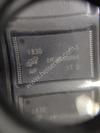
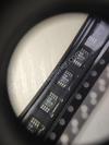
Part Number | MAX4495ASD+T |
---|---|
Manufacturer | Maxim Integrated |
Description | IC OPAMP GP 5MHZ RRO 14SOIC |
Datasheet | MAX4495ASD+T Datasheet |
Package | 14-SOIC (0.154", 3.90mm Width) |
In Stock | 10,300 piece(s) |
Unit Price | $ 1.5055 * |
Lead Time | Can Ship Immediately |
Estimated Delivery Time | Jan 24 - Jan 29 (Choose Expedited Shipping) |
Request for Quotation |
|
Part Number # MAX4495ASD+T (Linear - Amplifiers - Instrumentation, OP Amps, Buffer Amps) is manufactured by Maxim Integrated and distributed by Heisener. Being one of the leading electronics distributors, we carry many kinds of electronic components from some of the world’s top class manufacturers. Their quality is guaranteed by its stringent quality control to meet all required standards.
For MAX4495ASD+T specifications/configurations, quotation, lead time, payment terms of further enquiries please have no hesitation to contact us. To process your RFQ, please add MAX4495ASD+T with quantity into BOM. Heisener.com does NOT require any registration to request a quote of MAX4495ASD+T.
Manufacturer | Maxim Integrated |
Category | Integrated Circuits (ICs) - Linear - Amplifiers - Instrumentation, OP Amps, Buffer Amps |
Datasheet | MAX4495ASD+TDatasheet |
Package | 14-SOIC (0.154", 3.90mm Width) |
Series | - |
Amplifier Type | General Purpose |
Number of Circuits | 4 |
Output Type | Rail-to-Rail |
Slew Rate | 3 V/µs |
Gain Bandwidth Product | 5MHz |
-3db Bandwidth | - |
Current - Input Bias | 200nA |
Voltage - Input Offset | 300µV |
Current - Supply | 770µA |
Current - Output / Channel | 15mA |
Voltage - Supply, Single/Dual (±) | 4.5 V ~ 11 V, ��2.25 V ~ 5.5 V |
Operating Temperature | -40°C ~ 125°C |
Mounting Type | Surface Mount |
Package / Case | 14-SOIC (0.154", 3.90mm Width) |
Supplier Device Package | 14-SOIC |
For pricing, delivery, and ordering information, please contact Maxim Direct at 1-888-629-4642, or visit Maxim’s website at www.maxim-ic.com. General Description The MAX4493/MAX4494/MAX4495 single/dual/quad general-purpose operational amplifiers are designed for use in systems powered with dual supplies from ±2.25V to ±5.5V or with a single supply of +4.5V to +11V. These op amps provide a unity-gain bandwidth of 5MHz with only 770µA of quiescent current per amplifier. The wide input common-mode range extends from 200mV beyond the negative rail to within 1.5V of the positive supply rail while the output swings within 10mV (RL = 100kΩ) of either rail. These amplifiers have excellent (110dB) open-loop gain with very low THD+N of 0.002% (f = 1kHz). The single MAX4493 is available in a tiny 5-pin SC70 pack- age and the dual MAX4494 is available in the space- saving 8-pin SOT23. The quad MAX4495 is available in both 14-pin TSSOP and 14-pin SO packages. All prod- ucts are rated at the automotive temperature range of -40°C to +125°C. ________________________Applications Battery-Powered Systems DAC Output Amplifiers Industrial Control Systems Voltage Reference Generators Signal Conditioning Features 770µA Supply Current per Amplifier Operates from Dual ±2.25V to ±5.5V Supplies 5MHz Gain-Bandwidth Product Rail-to-Rail Output Swing Input Voltage Range Extends 200mV Below the Negative Rail 110dB Open-Loop Gain (RL = 100kΩ) Low THD+N of 0.002% (f = 1kHz) No Phase Reversal for Overdriven Inputs Unity-Gain Stable Available in Space-Saving Packages 5-Pin SC70 (MAX4493) 8-Pin SOT23 (MAX4494) 14-Pin TSSOP (MAX4495) M A X 4 4 9 3 /M A X 4 4 9 4 /M A X 4 4 9 5 SC70, Low-Power, General-Purpose, Dual-Supply, Rail-to-Rail Op Amps ________________________________________________________________ Maxim Integrated Products 1 VEE OUTIN- 1 + 5 VCCIN+ MAX4493 SC70/SOT23-5 TOP VIEW 2 3 4 Pin Configurations 19-1797; Rev 3; 12/09 Ordering Information Pin Configurations continued at end of data sheet. PART TEMP RANGE PIN- PACKAGE TOP MARK MAX4493AXK+T -40°C to +125°C 5 SC70 ABR MAX4493AXK/V+T -40°C to +125°C 5 SC70 +AUE MAX4493AUK+T -40°C to +125°C 5 SOT23 ADPG MAX4494AKA+T -40°C to +125°C 8 SOT23 AAEM MAX4494AKA/V+T -40°C to +125°C 8 SOT23 +AEQP MAX4494AUA+ -40°C to +125°C 8 µMAX — MAX4494ASA+ -40°C to +125°C 8 SO — MAX4495AUD+ -40°C to +125°C 14 TSSOP — MAX4495ASD+ -40°C to +125°C 14 SO — Typical Operating Characteristic TOTAL HARMONIC DISTORTION PLUS NOISE vs. FREQUENCY 1 100k10k1k10010 M A X 4 4 9 3 -0 8 FREQUENCY (Hz) TH D + N ( % ) 0 0.002 0.001 0.004 0.006 0.008 0.007 0.003 0.005 Typical Operating Circuit appears at end of data sheet. +Denotes a lead(Pb)-free/RoHS-compliant package. /V denotes an automotive qualified part. T = Tape and reel.
M A X 4 4 9 3 /M A X 4 4 9 4 /M A X 4 4 9 5 SC70, Low-Power, General-Purpose, Dual-Supply, Rail-to-Rail Op Amps 2 _______________________________________________________________________________________ ABSOLUTE MAXIMUM RATINGS DC ELECTRICAL CHARACTERISTICS (VCC = +5V, VEE = -5V, RL = 100kΩ to ground, TA = -40°C to +125°C. Typical values are at TA = +25°C, unless otherwise noted.) (Note 1) Stresses beyond those listed under “Absolute Maximum Ratings” may cause permanent damage to the device. These are stress ratings only, and functional operation of the device at these or any other conditions beyond those indicated in the operational sections of the specifications is not implied. Exposure to absolute maximum rating conditions for extended periods may affect device reliability. Supply Voltage (VCC to VEE)................................................+12V Voltage from Any Pin to Ground or Any Other Pin .............................(VEE - 0.3V) to (VCC + 0.3V) Output Short-Circuit Duration to VCC, VEE, or Ground ............................................Continuous Continuous Power Dissipation (TA = +70°C) 5-Pin SC70 (derate 3.1mW/°C above +70°C)............247mW 5-Pin SOT23 (derate 7.1mW/°C above +70°C)..........571mW 8-Pin SOT23 (derate 9.1mW/°C above +70°C)..........727mW 8-Pin µMAX® (derate 4.5mW/°C above +70°C) .........362mW 8-Pin SO (derate 5.9mW/°C above +70°C)................471mW 14-Pin TSSOP (derate 9.1mW/°C above +70°C) .......727mW 14-Pin SO (derate 8.3mW/°C above +70°C)..............667mW Operating Temperature Range .........................-40°C to +125°C Storage Temperature Range .............................-65°C to +150°C Lead Temperature (soldering, 10s) .................................+300°C PARAMETER SYMBOL CONDITIONS MIN TYP MAX UNITS Operating Supply Voltage Range VS Guaranteed by PSRR test ±2.25 ±5.5 V Quiescent Supply Current per Amplifier IS 770 1100 µA TA = +25°C 0.3 5 Input Offset Voltage VOS TA = TMIN to TMAX 10 mV Input Offset Voltage Drift TCVOS 3 µV/°C Input Offset Voltage Channel Matching MAX4494 and MAX4495 1 mV Input Bias Current IB 0.2 1 µA Input Offset Current IOS 5 300 nA Differential mode (-1V ≤ VIN ≤ +1V) 250 kΩ Input Resistance RIN Common mode (VEE - 0.2V ≤ VCM ≤ VCC - 1.5V) 110 MΩ Common-Mode Input Voltage Range VCM Guaranteed by CMRR test VEE - 0.2V VCC - 1.5V V Common-Mode Rejection Ratio CMRR VEE - 0.2V ≤ VCM ≤ VCC - 1.5V 65 90 dB Power-Supply Rejection Ratio PSRR VS = ±2.25V to ±5.5V 65 80 dB RL = 100kΩ, VEE + 0.25V ≤ VOUT ≤ VCC - 0.25V 85 110 Large-Signal Voltage Gain AVOL RL = 1kΩ, VEE + 0.5V ≤ VOUT ≤ VCC - 0.5V 65 90 dB RL = 100kΩ, VCC - VOH and VOL - VEE 10 150 Output Voltage Swing VOUT RL = 1kΩ, VCC - VOH and VOL - VEE 200 450 mV Output Short-Circuit Current ISC Sourcing or sinking 15 mA Note 1: All devices are 100% production tested at TA = +25°C. Limits over the operating temperature range are guaranteed by design and not production tested. µMAX is a registered trademark of Maxim Integrated products, Inc.
M A X 4 4 9 3 /M A X 4 4 9 4 /M A X 4 4 9 5 SC70, Low-Power, General-Purpose, Dual-Supply, Rail-to-Rail Op Amps _______________________________________________________________________________________ 3 AC ELECTRICAL CHARACTERISTICS (VCC = +5V, VEE = -5V, RL = 100kΩ to ground, CL = 15pF, TA = +25°C, unless otherwise noted.) PARAMETER SYMBOL CONDITIONS MIN TYP MAX UNITS Gain-Bandwidth Product GBWP 5 MHz Full-Power Bandwidth FPBW VOUT = 5Vp-p 190 kHz Slew Rate SR VOUT = 5Vp-p 3 V/µs Phase Margin 75 degrees Gain Margin 15 dB Total Harmonic Distortion Plus Noise THD+N f = 1kHz, VOUT = 5Vp-p, AV = +1V/V 0.002 % Settling Time to 0.01% tS AV = +1V/V, VOUT = 5V step 4 µs Input Capacitance CIN 2 pF Input Noise Voltage Density eIN f = 1kHz 8 nV/√Hz Input Noise Current Density iIN f = 1kHz 0.2 pA/√Hz All-Hostile Crosstalk f = 1kHz, MAX4494 and MAX4495 -100 dB Capacitive-Load Stability AV = +1V/V, no sustained oscillations 300 pF Power-Up Time tON VOUT = 1V, 1µs power supply rise-time 3 µs Typical Operating Characteristics (VCC = +5V, VEE = -5V, VCM = 0V, RL = 100kΩ to ground, CL = 15pF, TA = +25°C, unless otherwise noted.) 12575 10025 50-25 0-50 600 650 675 700 625 725 750 775 800 825 850 875 900 SUPPLY CURRENT vs. TEMPERATURE M A X 4 4 9 3 -0 1 TEMPERATURE (°C) S U P P LY C U R R EN T (μ A ) VSUPPLY = ±5V VSUPPLY = ±2.5V INPUT OFFSET VOLTAGE vs.TEMPERATURE M A X 4 4 9 3 -0 2 0 100 300 200 600 700 500 400 800 IN P U T O FF S ET V O LT A G E (μ V ) -50 0 25-25 50 75 100 125 TEMPERATURE (°C) INPUT BIAS CURRENT vs.TEMPERATURE M A X 4 4 9 3 -0 3 100 125 175 150 250 275 225 200 300 IN P U T B IA S C U R R EN T (n A ) -50 0 25-25 50 75 100 125 TEMPERATURE (°C)
M A X 4 4 9 3 /M A X 4 4 9 4 /M A X 4 4 9 5 SC70, Low-Power, General-Purpose, Dual-Supply, Rail-to-Rail Op Amps 4 _______________________________________________________________________________________ Typical Operating Characteristics (continued) (VCC = +5V, VEE = -5V, VCM = 0V, RL = 100kΩ to ground, CL = 15pF, TA = +25°C, unless otherwise noted.) 0 50 100 150 200 250 300 350 400 -5.0 -2.5 0 2.5 5.0 INPUT BIAS CURRENT vs. COMMON-MODE VOLTAGE M A X 4 4 9 3 -0 4 COMMON-MODE VOLTAGE (V) IN P U T B IA S C U R R EN T (n A ) VSUPPLY = ±2.5V VSUPPLY = ±5V COMMON-MODE REJECTION vs. FREQUENCY C O M M O N -M O D E R EJ EC TI O N ( dB ) -120 -80 -100 -40 -60 -20 0 1 10 100 1k 100k 1M M A X 4 4 9 3 -0 5 FREQUENCY (Hz) 10k 100 1k 10k 100k POWER-SUPPLY REJECTION vs. FREQENCY (VSUPPLY = ±2.5V to ±5.5V) M A X 4 4 9 3 -0 6 FREQUENCY (Hz) P O W ER S U P P LY R EJ EC TI O N ( dB ) -40 -100 -90 -80 -70 -60 -50 100 1 1 1k 10k 100k10 100 1M INPUT VOLTAGE NOISE DENSITY vs. FREQUENCY 10 M A X 4 4 9 3 -0 7 FREQUENCY (Hz) N O IS E D EN S IT Y ( nV /√ H z) TOTAL HARMONIC DISTORTION PLUS NOISE vs. FREQUENCY 1 100k10k1k10010 M A X 4 4 9 3 -0 8 FREQUENCY (Hz) TH D + N ( % ) 0 0.002 0.001 0.004 0.006 0.008 0.007 0.003 0.005 0 6 4 2 10 8 18 16 14 12 20 -50 -25 0 25 50 75 100 125 OUTPUT VOLTAGE SWING vs. TEMPERATURE (RL = 100kΩ) M A X 4 4 9 3 -0 9 TEMPERATURE (°C) O U TP U T V O LT A G E S W IN G ( m V ) VOL - VEE VCC - VOH 0 50 75 100 25 125 150 175 200 225 250 275 OUTPUT VOLTAGE SWING vs. TEMPERATURE (RL = 1kΩ) M A X 4 4 9 3 -1 0 TEMPERATURE (°C) O U TP U T V O LT A G E S W IN G ( m V ) -50 0 25-25 50 75 100 125 VCC - VOH VOL - VEE 40 60 100 80 120 140 -50 0-25 25 50 75 100 125 LARGE-SIGNAL GAIN vs. TEMPERATURE M A X 4 4 9 3 -1 1 TEMPERATURE (°C) LA R G E- S IG N A L G A IN ( dB ) RL = 100kΩ VEE + 0.25V ≤ VOUT ≤ VCC - 0.25V RL = 1kΩ VEE + 0.5V ≤ VOUT ≤ VCC - 0.5V 0.1k 1k 10k 100k 1M 10M 100M MAX4493-12 GAIN AND PHASE vs. FREQUENCY FREQUENCY (Hz) G A IN ( dB ) -60 -40 -20 -10 10 20 40 60 -50 -30 30 0 50 -270 -180 -90 -45 45 90 180 270 -225 -135 135 0 225 P H A S E (d eg re es ) GAIN PHASE AV = +1000V/V M A X 4 4 9 3 /M A X 4 4 9 4 /M A X 4 4 9 5
SC70, Low-Power, General-Purpose, Dual-Supply, Rail-to-Rail Op Amps _______________________________________________________________________________________ 5 G A IN ( dB ) GAIN AND PHASE vs. FREQUENCY (CL = 300pF) FREQUENCY (Hz) -60 -40 -20 -10 10 20 40 60 -50 -30 30 0 50 0.1k 1k 10k 100k 1M 10M 100M -270 -180 -90 -45 45 90 180 270 -225 -135 135 0 225 P H A S E (d eg re es ) MAX4493-13 AV = +1000V/V GAIN PHASE 80 90 85 100 95 110 120 105 115 8.8 9.2 9.49.0 9.6 9.8 10.0 LARGE-SIGNAL GAIN vs. OUTPUT VOLTAGE SWING (RL TO VCC, VCC = +5V, VEE = -5V) M A X 4 4 9 3 -1 4 TOTAL OUTPUT VOLTAGE SWING (VP-P) LA R G E- S IG N A L G A IN ( dB ) RL = 100kΩ RL = 1kΩ RL = 10kΩ 80 90 85 100 95 110 105 115 120 8.8 9.2 9.49.0 9.6 9.8 10.0 LARGE-SIGNAL GAIN vs. OUTPUT VOLTAGE SWING (RL TO VEE, VCC = +5V, VEE = -5V) M A X 4 4 9 3 -1 5 TOTAL OUTPUT VOLTAGE SWING (VP-P) LA R G E- S IG N A L G A IN ( dB ) RL = 100kΩ RL = 1kΩ RL = 10kΩ 3.4 3.83.6 4.0 4.2 4.4 RL = 100kΩ RL = 1kΩ RL = 10kΩ 70 80 75 90 85 100 95 105 115 110 120 LARGE-SIGNAL GAIN vs. OUTPUT VOLTAGE SWING (RL TO VCC, VCC = +2.25V, VEE = -2.25V) M A X 4 4 9 3 -1 6 TOTAL OUTPUT VOLTAGE SWING (VP-P) LA R G E- S IG N A L G A IN ( dB ) 3.4 3.83.6 4.0 4.2 4.4 RL = 100kΩ RL = 1kΩ RL = 10kΩ 70 80 75 90 85 100 95 105 110 115 LARGE-SIGNAL GAIN vs. OUTPUT VOLTAGE SWING (RL TO VEE, VCC = +2.25V, VEE = -2.25V) M A X 4 4 9 3 -1 7 TOTAL OUTPUT VOLTAGE SWING (VP-P) LA R G E- S IG N A L G A IN ( dB ) Typical Operating Characteristics (continued) (VCC = +5V, VEE = -5V, VCM = 0V, RL = 100kΩ to ground, CL = 15pF, TA = +25°C, unless otherwise noted.) M A X 4 4 9 3 /M A X 4 4 9 4 /M A X 4 4 9 5 LARGE-SIGNAL TRANSIENT RESPONSE M A X 4 4 9 3 -1 9 10μs/div INPUT VOLTAGE (2V/div) OUTPUT VOLTAGE (2V/div) 0 -120 10k 1M 10M100k MAX4494/MAX4495 CROSSTALK vs. FREQUENCY M A X 4 4 9 3 -1 8 FREQUENCY (Hz) C R O S S TA LK ( dB ) -100 -80 -60 -40 -20 M A X 4 4 9 3 /M A X 4 4 9 4 /M A X 4 4 9 5
M A X 4 4 9 3 /M A X 4 4 9 4 /M A X 4 4 9 5 SC70, Low-Power, General-Purpose, Dual-Supply, Rail-to-Rail Op Amps 6 _______________________________________________________________________________________ Typical Operating Characteristics (continued) (VCC = +5V, VEE = -5V, VCM = 0V, RL = 100kΩ to ground, CL = 15pF, TA = +25°C, unless otherwise noted.) SMALL-SIGNAL TRANSIENT RESPONSE 200ns/div IN P U T V O LT A G E (5 0m V /d iv ) O U TP U T V O LT A G E (5 0m V /d iv ) M A X 4 4 9 3 -2 0 LARGE-SIGNAL CAPACITIVE-LOAD STABILITY (CL = 1200pF) 10μs/div IN P U T V O LT A G E (2 V /d iv ) O U TP U T V O LT A G E (2 V /d iv ) M A X 4 4 9 3 -2 1 SMALL-SIGNAL CAPACITIVE-LOAD STABILITY (CL = 300pF) M A X 4 4 9 3 -2 2 200ns/div IN P U T V O LT A G E (5 0m V /d iv ) O U TP U T V O LT A G E (5 0m V /d iv ) SMALL-SIGNAL TRANSIENT RESPONSE (RISO = 15Ω, CL = 1000pF) M A X 4 4 9 3 -2 3 200ns/div IN P U T V O LT A G E (5 0m V /d iv ) O U TP U T V O LT A G E (5 0m V /d iv ) LARGE-SIGNAL TRANSIENT RESPONSE (RISO = 15Ω, CL = 0.01μF) M A X 4 4 9 3 -2 4 10μs/div IN P U T V O LT A G E (2 V /d iv ) O U TP U T V O LT A G E (2 V /d iv ) POWER-UP TIME (VIN = +1V) M A X 4 4 9 3 -2 5 10μs/div VCC - VEE (4V/div) OUTPUT VOLTAGE (500mV/div) 10 0 1V 0 1000 0 1k 10k 100k STABILITY vs. CAPACITIVE AND RESISTIVE LOADS 200 100 M A X 4 4 9 3 -2 6 RLOAD (Ω) C LO A D ( pF ) 400 300 600 700 500 800 900 STABLE REGION M A X 4 4 9 3 /M A X 4 4 9 4 /M A X 4 4 9 5
M A X 4 4 9 3 /M A X 4 4 9 4 /M A X 4 4 9 5 SC70, Low-Power, General-Purpose, Dual-Supply, Rail-to-Rail Op Amps _______________________________________________________________________________________ 7 Pin Description PIN MAX4493 MAX4494 MAX4495 NAME FUNCTION — 1 1 OUTA Channel A Output — 2 2 INA- Channel A Inverting Input — 3 3 INA+ Channel A Noninverting Input — 7 7 OUTB Channel B Output — 6 6 INB- Channel B Inverting Input — 5 5 INB+ Channel B Noninverting Input — — 8 OUTC Channel C Output — — 9 INC- Channel C Inverting Input — — 10 INC+ Channel C Noninverting Input — — 14 OUTD Channel D Output — — 13 IND- Channel D Inverting Input — — 12 IND+ Channel D Noninverting Input 4 — —- OUT Output 1 — — IN+ Noninverting Input 3 — — IN- Inverting Input 5 8 4 VCC Positive Supply 2 4 11 VEE Negative Supply Applications Information Rail-to-Rail Output Stage The MAX4493/MAX4494/MAX4495 output stage can drive up to 1kΩ and still swing within 200mV of the rails. Capacitive-Load Stability Driving large capacitive loads can cause instability in many op amps. The MAX4493/MAX4494/MAX4495 are stable with capacitive loads up to 300pF. The Capacitive-Load Stabil i ty graph in the Typical Operating Characteristics gives the stable operation region for capacitive versus resistive load. Stability with higher capacitive loads can be improved by adding an isolation resistor in series with the op-amp output, as shown in Figure 1. This resistor improves the circuit’s phase margin by isolating the load capacitor from the amplifier’s output. As seen in the Typical Operating Characteristics, driving capacitive loads with an isola- tion resistor exhibits some overshoot, but no oscillation. Full-Power Bandwidth The FPBW is given by: FPBW Hz SR VOUTp p ( ) (max) = [ ]−π RISO INPUT OUTPUT CL MAX4493 Figure 1. Capacitive Load Driving Circuit
M A X 4 4 9 3 /M A X 4 4 9 4 /M A X 4 4 9 5 where the slew rate (SR) is 3V/µs. Figure 2 shows thefull-power bandwidth as a function of the peak-to-peak AC output voltage. Power-Up Conditions The MAX4493/MAX4494/MAX4495 typically settle within 3µs after power-up. See Power-Up Time in Typical Operating Characteristics. Power Supplies and Layout The MAX4493/MAX4494/MAX4495 operate with dual supplies from ±2.25V to ±5.5V. Bypass both VCC and VEE with their own 0.1µF capacitor to ground. Good layout technique helps optimize performance by decreasing the amount of stray capacitance at the op amp’s inputs and outputs. To decrease stray capaci- tance, minimize trace lengths by placing external com- ponents close to the op amp’s pins. SC70, Low-Power, General-Purpose, Dual-Supply, Rail-to-Rail Op Amps 8 _______________________________________________________________________________________ Chip Information PROCESS: Bipolar 14 13 12 11 10 9 8 1 2 3 4 5 6 7 OUTD IND- IND+ VEEVCC INA+ INA- OUTA TOP VIEW MAX4495 INC+ INC- OUTCOUTB INB- INB+ SO/TSSOP Pin Configurations (continued) INB- INB+VEE 1 2 8 7 VCC OUTBINA- INA+ OUTA SO/SOT23/μMAX TOP VIEW 3 4 6 5 MAX4494 -5V +5V VOUT RISO -5V 0.1μF 0.1μF0.1μF 0.1μF +5V RfRg REF DAC MAX4493 Typical Operating Circuit 0 21 3 5 BANDWIDTH vs. OUTPUT VOLTAGE SWING VOUT (Vp-p) B A N D W ID TH ( H z) 100M 100k 1M 10M 4 AV = +1V/V Figure 2. Bandwidth vs. Peak-to-Peak AC Voltage Plot
M A X 4 4 9 3 /M A X 4 4 9 4 /M A X 4 4 9 5 SC70, Low-Power, General-Purpose, Dual-Supply, Rail-to-Rail Op Amps _______________________________________________________________________________________ 9 T S S O P 4 .4 0 m m .E P S PACKAGE TYPE PACKAGE CODE DOCUMENT NO. 14 TSSOP U14-1 21-0066 5 SOT23 U5-1 21-0057 5 SC70 X5-1 21-0076 8 SO S8-2 21-0041 8 SOT23 K8-5 21-0078 8 µMAX U8-1 21-0036 14 SO S14-1 21-0041 Package Information For the latest package outline information and land patterns, go to www.maxim-ic.com/packages. Note that a “+”, “#”, or “-” in the package code indicates RoHS status only. Package drawings may show a different suffix character, but the drawing pertains to the package regardless of RoHS status.
Cann*****adan
December 23, 2020
Lila*****averi
December 17, 2020
Mada*****Saha
December 13, 2020
Sie*****Byrd
December 12, 2020
Rive*****ndal
December 4, 2020
Dako*****rince
November 30, 2020
Jour*****Mckay
November 30, 2020
We guarantee 100% customer satisfaction.
Our experienced sales team and tech support team back our services to satisfy all our customers.
We provide 90 days warranty.
If the items you received were not in perfect quality, we would be responsible for your refund or replacement, but the items must be returned in their original condition.
Payment Methods | |
Delivery Services |
Heisener's commitment to quality has shaped our processes for sourcing, testing, shipping, and every step in between. This foundation underlies each component we sell.