Part Number | MAX4521ESE+T |
---|---|
Manufacturer | Maxim Integrated |
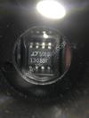
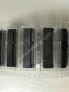
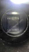
Description | IC SWITCH QUAD SPST 16SOIC |
Datasheet | MAX4521ESE+T Datasheet |
Package | 16-SOIC (0.154", 3.90mm Width) |
In Stock | 7,420 piece(s) |
Unit Price | $ 1.2974 * |
Lead Time | Can Ship Immediately |
Estimated Delivery Time | Jan 24 - Jan 29 (Choose Expedited Shipping) |
Request for Quotation |
|
Part Number # MAX4521ESE+T (Interface - Analog Switches, Multiplexers, Demultiplexers) is manufactured by Maxim Integrated and distributed by Heisener. Being one of the leading electronics distributors, we carry many kinds of electronic components from some of the world’s top class manufacturers. Their quality is guaranteed by its stringent quality control to meet all required standards.
For MAX4521ESE+T specifications/configurations, quotation, lead time, payment terms of further enquiries please have no hesitation to contact us. To process your RFQ, please add MAX4521ESE+T with quantity into BOM. Heisener.com does NOT require any registration to request a quote of MAX4521ESE+T.
Manufacturer | Maxim Integrated |
Category | Integrated Circuits (ICs) - Interface - Analog Switches, Multiplexers, Demultiplexers |
Datasheet | MAX4521ESE+TDatasheet |
Package | 16-SOIC (0.154", 3.90mm Width) |
Series | - |
Switch Circuit | SPST - NC |
Multiplexer/Demultiplexer Circuit | 1:1 |
Number of Circuits | 4 |
On-State Resistance (Max) | 100 Ohm |
Channel-to-Channel Matching (ΔRon) | 1 Ohm |
Voltage - Supply, Single (V+) | 2 V ~ 12 V |
Voltage - Supply, Dual (V±) | ��2 V ~ 6 V |
Switch Time (Ton, Toff) (Max) | 80ns, 30ns |
-3db Bandwidth | - |
Charge Injection | 1pC |
Channel Capacitance (CS(off), CD(off)) | 2pF, 2pF |
Current - Leakage (IS(off)) (Max) | 1nA |
Crosstalk | -90dB @ 100kHz |
Operating Temperature | -40°C ~ 85°C (TA) |
Package / Case | 16-SOIC (0.154", 3.90mm Width) |
Supplier Device Package | 16-SO |
General Description The MAX4521/MAX4522/MAX4523 are quad, low-volt- age, single-pole/single-throw (SPST) analog switches. On-resistance (100Ω max) is matched between switch- es to 4Ω max, and is flat (12Ω max) over the specified signal range. Each switch can handle rail-to-rail analog signals. The off-leakage current is only 1nA at +25°C and 10nA at +85°C. The MAX4521 has four normally closed (NC) switches, and the MAX4522 has four normally open (NO) switch- es. The MAX4523 has two NC switches and two NO switches. These CMOS switches can operate with dual power supplies ranging from ±2V to ±6V or a single supply between +2V and +12V. They are fully specified for sin- gle +2.7V operation. All digital inputs have +0.8V and +2.4V logic thresh- olds, ensuring TTL/CMOS-logic compatibility when using ±5V or a single +5V supply. Applications Battery-Operated Equipment Data Acquisition Test Equipment Avionics Audio Signal Routing Networking Features ♦ +2V to +12V Single Supply ±2V to ±6V Dual Supplies ♦ 100Ω Signal Paths with ±5V Supplies ♦ Low Power Consumption, <1µW ♦ 4 Separately Controlled SPST Switches ♦ Rail-to-Rail Signal Handling ♦ Pin Compatible with Industry-Standard DG211/DG212/DG213 ♦ >2kV ESD Protection per Method 3015.7 ♦ TTL/CMOS-Compatible Inputs with ±5V or Single +5V Supply M A X 4 5 2 1 /M A X 4 5 2 2 /M A X 4 5 2 3 Quad, Low-Voltage, SPST Analog Switches ________________________________________________________________ Maxim Integrated Products 1 SWITCHES SHOWN FOR LOGIC "0" INPUT DIP/SO/QSOP/TSSOP MAX4522 LOGIC SWITCH 0 1 OFF ON TOP VIEW DIP/SO/QSOP/TSSOP MAX4521 LOGIC SWITCH 0 1 ON OFF DIP/SO/QSOP/TSSOP MAX4523 LOGIC SWITCHES 1, 4 0 1 OFF ON SWITCHES 2, 3 ON OFF 16 15 14 13 12 11 10 9 1 2 3 4 5 6 7 8 IN2 COM2 NC2 V+V- NO1 COM1 IN1 MAX4523 N.C. NC3 COM3 IN3IN4 COM4 NO4 GND 16 15 14 13 12 11 10 9 1 2 3 4 5 6 7 8 IN2 COM2 NC2 V+V- NC1 COM1 IN1 MAX4521 N.C. NC3 COM3 IN3IN4 COM4 NC4 GND 16 15 14 13 12 11 10 9 1 2 3 4 5 6 7 8 IN2 COM2 NO2 V+V- NO1 COM1 IN1 MAX4522 N.C. NO3 COM3 IN3IN4 COM4 NO4 GND N.C. = NOT CONNECTED Pin Configurations/Functional Diagrams/Truth Tables 19-1136; Rev 6; 7/07 Ordering Information Ordering Information continued at end of data sheet. *Contact factory for dice specifications. **EP = Exposed pad. For pricing, delivery, and ordering information, please contact Maxim Direct at 1-888-629-4642, or visit Maxim’s website at www.maxim-ic.com. Pin Configurations continued at end of data sheet. PART TEMP RANGE PIN- PACKAGE PKG CODE MAX4521CPE 0°C to +70°C 16 Plastic DIP P16-1 MAX4521CSE 0°C to +70°C 16 Narrow SO S16-2 MAX4521CEE 0°C to +70°C 16 QSOP E16-4 MAX4521CUE 0°C to +70°C 16 TSSOP U16-2 MAX4521CGE 0°C to +70°C 16 QFN-EP** G1644-1 MAX4521C/D 0°C to +70°C Dice* —
M A X 4 5 2 1 /M A X 4 5 2 2 /M A X 4 5 2 3 Quad, Low-Voltage, SPST Analog Switches 2 _______________________________________________________________________________________ ABSOLUTE MAXIMUM RATINGS ELECTRICAL CHARACTERISTICS—Dual Supplies (V+ = +4.5V to +5.5V, V- = -4.5V to -5.5V, TA = TMIN to TMAX, unless otherwise noted. Typical values are at TA = +25°C.) Note 1: Signals on NC_, NO_, COM_, or IN_ exceeding V+ or V- are clamped by internal diodes. Limit forward-diode current to maxi- mum current rating. Note 2: All leads are soldered or welded to PC boards. Stresses beyond those listed under “Absolute Maximum Ratings” may cause permanent damage to the device. These are stress ratings only, and functional operation of the device at these or any other conditions beyond those indicated in the operational sections of the specifications is not implied. Exposure to absolute maximum rating conditions for extended periods may affect device reliability. Voltages Referenced to GND V+.....................................................................-0.3V to +13.0V V- .....................................................................-13.0V to +0.3V V+ to V- ............................................................-0.3V to +13.0V All Other Pins (Note 1) ..........................(V- - 0.3V) to (V+ + 0.3V) Continuous Current into Any Terminal..............................±10mA Peak Current into Any Terminal (pulsed at 1ms,10% duty cycle)...................................±20mA ESD per Method 3015.7 ..................................................>2000V Continuous Power Dissipation (TA = +70°C) (Note 2) Plastic DIP (derate 10.53mW/°C above +70°C) ..........842mW Narrow SO (derate 8.70mW/°C above +70°C) ............696mW QSOP (derate 9.52mW/°C above +70°C)....................762mW CERDIP (derate 10.00mW/°C above +70°C)...............800mW TSSOP (derate 6.7mW/°C above +70°C) ....................457mW QFN (derate 16.9mW/°C above +70°C) ....................1349mW Operating Temperature Ranges MAX452_C_E ......................................................0°C to +70°C MAX452_E_E ...................................................-40°C to +85°C MAX452_MJE ................................................-55°C to +125°C Storage Temperature Range .............................-65°C to +150°C Lead Temperature (soldering, 10s) .................................+300°C (Note 4) V+ = 5.5V, V- = -5.5V, VCOM_ = ±4.5V V+ = 5.5V, V- = -5.5V, VCOM_ = ±4.5V, VN_ = 4.5V V+ = 5V, V- = -5V, VCOM_ = ±3V, ICOM_ = 1mA V+ = 5.5V, V- = -5.5V, VCOM_ = 4.5V, VN_ = ±4.5V V+ = 5V, V- = -5V, VCOM_ = ±3V, ICOM_ = 1mA V+ = 5V, V- = -5V, VCOM_ = ±3V, ICOM_ = 1mA CONDITIONS nA -200 200 ICOM_(ON) COM_ On-Leakage Current (Note 7) -20 20 -2 0.01 2 nA -100 100 ICOM_(OFF) COM_ Off-Leakage Current (Note 7) -10 10 -1 0.01 1 nA -100 100 INO_(OFF), INC_(OFF) NO_, NC_ Off-Leakage Current (Note 7) -10 10 -1 0.01 1 VV- V+ VCOM_, VNO_, VNC_ Analog Signal Range Ω 15 RFLAT(ON) COM_ to NO_, COM_ to NC_ On-Resistance Flatness (Note 6) 7 12 Ω 6 ΔRON COM_ to NO_, COM_ to NC_ On-Resistance Match Between Channels (Note 5) 65 100 Ω 125 RON COM_ to NO_, COM_ to NC_ On-Resistance 1 4 UNITS MIN TYP MAX (Note 3) SYMBOLPARAMETER C, E, M M C, E +25°C M C, E C, E, M +25°C M +25°C C, E, M +25°C C, E, M +25°C C, E +25°C TA ANALOG SWITCH ± ±
M A X 4 5 2 1 /M A X 4 5 2 2 /M A X 4 5 2 3 Quad, Low-Voltage, SPST Analog Switches _______________________________________________________________________________________ 3 ELECTRICAL CHARACTERISTICS—Dual Supplies (continued) (V+ = +4.5V to +5.5V, V- = -4.5V to -5.5V, TA = TMIN to TMAX, unless otherwise noted. Typical values are at TA = +25°C.) CONDITIONS C, E, M C, E, M V0.8 1.6VIN_LIN_ Input Logic Threshold Low V1.6 2.4VIN_HIN_ Input Logic Threshold High UNITS MIN TYP MAX (Note 3) SYMBOLPARAMETER TA C, E, MVIN_ = 0.8V or 2.4V µA-1 0.03 1IINH_, IINL_ IN_ Input Current Logic High or Low +25°C 45 80 Turn-On Time tON VCOM_ = ±3V, V+ = 4.5V, V- = -4.5V, Figure 1 C, E, M 100 ns +25°C 15 30 Turn-Off Time tOFF VCOM_ = ±3V, V+ = 4.5V, V- = -4.5V, Figure 1 C, E, M 40 ns Break-Before-Make Time Delay (MAX4523 only) tBBM VCOM_ = ±3V, V+ = 5.5V, V- = -5.5V, Figure 2 +25°C 5 20 ns Charge Injection (Note 4) Q CL = 1nF, VNO_ = 0, RS = 0Ω, Figure 3 +25°C 1 5 pC NO_, NC_ Off-Capacitance CN_(OFF) VNO_ = GND, f = 1MHz, Figure 6 +25°C 2 pF COM_ Off-Capacitance CCOM_(OFF) VCOM_ = GND, f = 1MHz, Figure 6 +25°C 2 pF COM_ On-Capacitance CCOM_(ON) VCOM_ = VNO_ = GND, f = 1MHz, Figure 7 +25°C 5 pF Off-Isolation (Note 8) VISO RL = 50Ω, CL = 15pF, VN_ = 1VRMS, f = 100kHz, Figure 4 +25°C < -90 dB Power-Supply Range V+, V- C, E, M -6 6 V -1 0.05 1 V+ Supply Current I+ V+ = 5.5V, all VIN_ = 0 or V+ C, E, M -1 1 µA +25°C -1 0.05 1 V- Supply Current I- V- = -5.5V C, E, M -1 1 µA +25°C Channel-to-Channel Crosstalk (Note 9) VCT RL = 50Ω, CL = 15pF, VN_ = 1VRMS, f = 100kHz, Figure 5 +25°C < -90 dB POWER SUPPLY LOGIC INPUT SWITCH DYNAMIC CHARACTERISTICS
M A X 4 5 2 1 /M A X 4 5 2 2 /M A X 4 5 2 3 Quad, Low-Voltage, SPST Analog Switches 4 _______________________________________________________________________________________ ELECTRICAL CHARACTERISTICS—Single +5V Supply (V+ = +4.5V to +5.5V, V- = 0V, TA = TMIN to TMAX, unless otherwise noted. Typical values are at TA = +25°C.) +25°C (Note 4) CONDITIONS C, E, M 125 200 V0 V+ VCOM_, VNO_, VNC_ Analog Signal Range UNITS MIN TYP MAX (Note 3) SYMBOLPARAMETER TA COM_ to NO_, COM_ to NC_ On-Resistance RON V+ = 4.5V, VCOM_ = 3.5V, ICOM_ = 1mA C, E, M 250 Ω +25°C 2 8COM_ to NO_, COM_ to NC_ On-Resistance Match Between Channels (Note 5) ΔRON V+ = 5V, VCOM_ = 3.5V, ICOM_ = 1mA C, E, M 10 Ω +25°C -1 0.01 1 C, E -10 10 NO_, NC_ Off-Leakage Current (Notes 7, 10) INO_(OFF), INC_(OFF) V+ = 5.5V; VCOM_ = 1V, 4.5V; VN_ = 4.5V, 1V M -100 100 nA +25°C -1 0.01 1 C, E -10 10 COM_ Off-Leakage Current (Notes 7, 10) ICOM_(OFF) V+ = 5.5V; VCOM_ = 1V, 4.5V; VN_ = 4.5V, 1V M -100 100 nA +25°C -2 0.01 2 C, E, -20 20 COM_ On-Leakage Current (Notes 7, 10) ICOM_(ON) V+ = 5.5V; VCOM_ = 4.5V, 1V M -200 200 nA IN_ Input Logic Threshold High VIN_H C, E 1.6 2.4 V IN_ Input Logic Threshold Low VIN_L C, E 0.8 1.6 V IN_ Input Current Logic High or Low IINH_, IINL_ VIN_ = 0.8V or 2.4V C, E -1 0.03 1 µA +25°C 60 100 Turn-On Time tON VCOM_ = 3V, V+ = 4.5V, Figure 1 C, E, M 150 ns +25°C 20 50 Turn-Off Time tOFF VCOM_ = 3V, V+ = 4.5V, Figure 1 C, E, M 75 ns +25°C 10 30 Break-Before-Make Time Delay (MAX4523 only) tBBM VCOM_ = 3V, V+ = 5.5V, Figure 2 ns +25°C -1 0.05 1 V+ Supply Current I+ V+ = 5.5V, all VIN_ = 0 or V+ C, E, M -1 1 µA +25°C -1 0.05 1 V- Supply Current I- V- = 0 C, E, M -1 1 µA Charge Injection (Note 4) Q CL = 1nF, VNO_ = 0, RS = 0Ω, Figure 3 +25°C 1 5 pC POWER SUPPLY SWITCH DYNAMIC CHARACTERISTICS LOGIC INPUT ANALOG SWITCH
M A X 4 5 2 1 /M A X 4 5 2 2 /M A X 4 5 2 3 Quad, Low-Voltage, SPST Analog Switches _______________________________________________________________________________________ 5 Note 3: The algebraic convention is used in this data sheet; the most negative value is shown in the minimum column. Note 4: Guaranteed by design. Note 5: ΔRON = ΔRON(MAX) - ΔRON(MIN). Note 6: Resistance flatness is defined as the difference between the maximum and minimum on-resistance values, as measured over the specified analog signal range. Note 7: Leakage parameters are 100% tested at maximum rated temperature, and guaranteed by correlation at TA = +25°C. Note 8: Off-Isolation = 20log10 [ VCOM_ / (VNC_ or VNO_) ], VCOM_ = output, VNC_ or VNO_ = input to off switch. Note 9: Between any two switches. Note 10: Leakage testing for single-supply operation is guaranteed by testing with dual supplies. ELECTRICAL CHARACTERISTICS—Single +3V Supply (V+ = +2.7V to +3.6V, V- = 0V, TA = TMIN to TMAX, unless otherwise noted. Typical values are at TA = +25°C.) +25°C (Note 4) COM_ to NO_, COM_ to NC_ On-Resistance RON V+ = 2.7V, VCOM_ = 1.0V, ICOM_ = 0.1mA C, E, M 600 Ω IN_ Input Logic Threshold High VIN_H C, E 1.6 2.4 V IN_ Input Logic Threshold Low CONDITIONS C, E, M VIN_L 260 500 V0 V+ VCOM_, VNO_, VNC_ Analog Signal Range C, E 0.8 1.6 V IN_ Input Current Logic High or Low IINH_, IINL_ VIN_ = 0.8V or 2.4V C, E -1 0.03 1 µA +25°C 120 250 Turn-On Time tON VCOM_ = 1.5V, V+ = 2.7V, Figure 1 C, E, M 300 ns +25°C 40 80 Turn-Off Time tOFF VCOM_ = 1.5V, V+ = 2.7V, Figure 1 C, E, M 100 ns +25°C 15 50 Break-Before-Make Time Delay (MAX4523 only) tBBM VCOM_ = 1.5V, V+ = 3.6V, Figure 2 ns +25°C -1 0.05 1 V+ Supply Current UNITS MIN TYP MAX (Note 3) SYMBOLPARAMETER I+ V+ = 3.6V, all VIN_ = 0 or V+ C, E, M -1 1 µA +25°C -1 0.05 1 V- Supply Current I- V- = 0 C, E, M -1 1 µA TA Charge Injection Q CL = 1nF, VNO_ = 0, RS = 0Ω, Figure 3 +25°C 0.5 5 pC ANALOG SWITCH LOGIC INPUT SWITCH DYNAMIC CHARACTERISTICS (Note 4) POWER SUPPLY
M A X 4 5 2 1 /M A X 4 5 2 2 /M A X 4 5 2 3 Quad, Low-Voltage, SPST Analog Switches 6 _______________________________________________________________________________________ Typical Operating Characteristics (V+ = +5V, V- = -5V, GND = 0, TA = +25°C, unless otherwise noted.) 100 0 -5 -3 1 5 ON-RESISTANCE vs. VCOM (DUAL SUPPLIES) 20 80 M A X 4 5 2 1 /2 /3 -T O C 0 1 VCOM (V) R O N ( Ω ) -1 3-4 -2 20 4 60 160 180 140 120 40 V+, V- = 2.0V V+, V- = 3.0V V+, V- = 4.0V V+, V- = 5.0V 80 30 -5 -3 1 5 ON-RESISTANCE vs. VCOM AND TEMPERATURE (DUAL SUPPLIES) 40 70 M A X 4 5 2 1 /2 /3 -T O C 0 2 VCOM (V) R O N ( Ω ) -1 3-4 -2 20 4 60 110 100 90 50 TA = +125°C TA = +85°C TA = +25°C TA = 0°C TA = -55°C 250 0 0 1 3 5 ON-RESISTANCE vs. VCOM (SINGLE SUPPLY) 50 200 M A X 4 5 2 1 /2 /3 -T O C 0 3 VCOM (V) R O N ( Ω ) 2 4 150 350 300 100 V+ = 2.7V V+ = 3.3V V+ = 5.0V 160 60 0 1 3 5 ON-RESISTANCE vs. VCOM AND TEMPERATURE (SINGLE SUPPLY) 80 140 M A X 4 5 2 1 /2 /3 -T O C 0 4 VCOM (V) R O N ( Ω ) 2 4 120 200 180 100 TA = +25°C TA = +125°C TA = +85°C TA = 0°C TA = -55°C 200 0 2 4 8 12 TURN-ON/OFF TIME vs. SUPPLY VOLTAGE 40 160 tON tOFF M A X 4 5 2 1 /2 /3 -T O C 0 7 t O N , t O FF ( n s) V+ (V) 6 103 7 115 9 120 80 180 20 140 100 60 10n 0.1p -55 -25 0 25 75 ON- AND OFF-LEAKAGE CURRENT vs. TEMPERATURE 1p 1n MA X 4 5 2 1 /2 /3 -T O C 0 5 TEMPERATURE (°C) L E A K A G E C U R R E N T ( A ) 50 100 125 100p 10p ON LEAKAGE OFF LEAKAGE 2 -2 -5 -3 1 5 CHARGE INJECTION vs. VCOM 1 M A X 4 5 2 1 /2 /3 -T O C 0 6 VCOM (V) Q ( p C ) -1 3-4 -2 20 4 0 -1 V+ = +5V V- = 0V V+ = +5V V- = -5V 100 0 -55 -25 75 TURN-ON/OFF TIME vs. TEMPERATURE 20 80 tON tOFF M A X 4 5 2 1 /2 /3 -T O C 0 8 TEMPERATURE (°C) t O N , t O FF ( n s) 25 500 125100 60 40 90 10 70 50 30 1 0.00001 -55 -25 75 POWER-SUPPLY CURRENT vs. TEMPERATURE 0.0001 0.1 I+ I- M A X 4 5 2 1 /2 /3 -T O C 0 9 TEMPERATURE (°C) I+ , I- ( μA ) 25 500 125100 0.01 0.001
M A X 4 5 2 1 /M A X 4 5 2 2 /M A X 4 5 2 3 Quad, Low-Voltage, SPST Analog Switches _______________________________________________________________________________________ 7 100 0.001 10 1k100 100k10k TOTAL HARMONIC DISTORTION vs. FREQUENCY 0.01 M A X 4 5 2 1 /2 /3 -T O C 1 0 FREQUENCY (Hz) T H D ( % ) 0.1 1 10 V+ = +5V V- = -5V 600Ω IN AND OUT 0 -10 -90 0.01 0.1 1 10 100 300 FREQUENCY RESPONSE -80 -70 M A X 4 5 2 1 /2 /3 -T O C 1 1 FREQUENCY (MHz) L O S S ( d B ) P H A S E ( D E G R E E S ) -50 -60 -40 -20 -30 5 0 -40 -35 -30 -20 -25 -15 -5 -10 INSERTION LOSS 50Ω IN/OUT OFF-ISOLATION ON-PHASE Typical Operating Characteristics (continued) (V+ = +5V, V- = -5V, GND = 0, TA = +25°C, unless otherwise noted.) Pin Description *NO_ (or NC_) and COM_ pins are identical and interchangeable. Either may be considered as an input or output; signals pass equally well in either direction. PIN MAX4521 MAX4522 MAX4523 TSSOP/SO QFN TSSOP/SO QFN TSSOP/SO QFN NAME FUNCTION 1, 16, 9, 8 15, 14, 7, 6 1, 16, 9, 8 15, 14, 7, 6 1, 16, 9, 8 15, 14, 7, 6 IN1–1N4 Logic-Control Digital Input 2, 15, 10, 7 16, 13, 8, 5 2, 15, 10, 7 16, 13, 8, 5 2, 15, 10, 7 16, 13, 8, 5 COM1–COM4 Analog Switch Common* Terminals 3, 14, 11, 6 1, 12, 9, 4 — — — — NC1–NC4 Analog Switch Normally Closed Terminals — — 3, 14, 11, 6 1, 12, 9, 4 — — NO1–NO4 Analog Switch Normally Open Terminals — — — — 3, 6 1, 4 NO1, NO4 Analog Switch Normally Open Terminals — — — — 14, 11 12, 9 NC2, NC3 Analog Switch Normally Closed Terminals 4 2 4 2 4 2 V- Negative Analog Supply-Voltage Input. Connect to GND for single supply operation. 5 3 5 3 5 3 GND Ground. Connect to digital ground. (Analog signals have no ground reference; they are limited to V+ and V-.) 12 10 12 10 12 10 N.C. No Connection. Not internally connected. 13 11 13 11 13 11 V+ Positive Analog and Digital Supply- Voltage Input. Internally connected to substrate. — EP — EP — EP EP Exposed Pad. Connect EP to V+.
M A X 4 5 2 1 /M A X 4 5 2 2 /M A X 4 5 2 3 Applications Information Power-Supply Considerations Overview The MAX4521/MAX4522/MAX4523 construction is typi- cal of most CMOS analog switches. They have three supply pins: V+, V-, and GND. V+ and V- are used to drive the internal CMOS switches, and they set the lim- its of the analog voltage on any switch. Reverse ESD- protection diodes are internally connected between each analog-signal pin and both V+ and V-. If any ana- log signal exceeds V+ or V-, one of these diodes con- ducts. During normal operation these reverse-biased ESD diodes leak, forming the only current drawn from V+ or V-. Virtually all the analog leakage current is through the ESD diodes. Although the ESD diodes on a given sig- nal pin are identical and therefore fairly well balanced, they are reverse biased differently. Each is biased by either V+ or V- and the analog signal. This means their leakages vary as the signal varies. The difference in the two diode leakages from the signal path to the V+ and V- pins constitutes the analog-signal-path leakage cur- rent. All analog leakage current flows to the supply ter- minals, not to the other switch terminal. This explains how both sides of a given switch can show leakage currents of the same or opposite polarity. There is no connection between the analog-signal paths and GND. The analog-signal paths consist of an N-channel and P-channel MOSFET with their sources and drains paralleled, and their gates driven out of phase to V+ and V- by the logic-level translators. V+ and GND power the internal logic and logic-level translators, and set the input logic thresholds. The logic-level translators convert the logic levels to switched V+ and V- signals to drive the gates of the analog switches. This drive signal is the only connec- tion between the logic supplies and the analog sup- plies. V+ and V- have ESD-protection diodes to GND. The logic-level inputs and output have ESD protection to V+ and to GND. Increasing V- has no effect on the logic-level thresh- olds, but it does increase the drive to the P-channel switches, reducing their on-resistance. V- also sets the negative limit of the analog-signal voltage. The logic-level thresholds are CMOS/TTL compatible when V+ = +5V. The threshold increases slightly as V+ is raised, and when V+ reaches +12V, the level thresh- old is about 3.1V. This is above the TTL output high- level minimum of 2.8V, but still compatible with CMOS outputs. Bipolar Supplies The MAX4521/MAX4522/MAX4523 operate with bipolar supplies between ±2V and ±6V. The V+ and V- sup- plies need not be symmetrical, but their sum cannot exceed the absolute maximum rating of 13.0V. Do not connect the MAX4521/MAX4522/MAX4523 V+ to +3V, and then connect the logic-level-input pins to TTL logic-level signals. TTL logic-level outputs in excess of the absolute maximum ratings can damage the part and/or external circuits. Caution: The absolute maximum V+ to V- differential voltage is 13.0V. Typical ±6V or 12V supplies with ±10% tolerances can be as high as 13.2V. This voltage can damage the MAX4521/MAX4522/MAX4523. Even ±5% tolerance supplies may have overshoot or noise spikes that exceed 13.0V. Single Supply The MAX4521/MAX4522/MAX4523 operate from a single supply between +2V and +12V when V- is con- nected to GND. All of the bipolar precautions must be observed. High-Frequency Performance In 50Ω systems, signal response is reasonably flat up to 50MHz (see Typical Operating Characteristics). Above 20MHz, the on-response has several minor peaks that are highly layout dependent. The problem with high-frequency operation is not turning the switch on, but turning it off. The off-state switch acts like a capacitor and passes higher frequencies with less attenuation. At 10MHz, off-isolation is about -52dB in 50Ω systems, becoming worse (approximately 20dB per decade) as frequency increases. Higher circuit impedances also make off-isolation worse. Adjacent channel attenuation is about 3dB above that of a bare IC socket, and is due entirely to capacitive coupling. Quad, Low-Voltage, SPST Analog Switches 8 _______________________________________________________________________________________
M A X 4 5 2 1 /M A X 4 5 2 2 /M A X 4 5 2 3 Quad, Low-Voltage, SPST Analog Switches _______________________________________________________________________________________ 9 VGEN GND NC or NO CL VOUT V- V- V+ VOUT IN OFF ON OFF ΔVOUT Q = (ΔVOUT)(CL) COM IN DEPENDS ON SWITCH CONFIGURATION; INPUT POLARITY DETERMINED BY SENSE OF SWITCH. OFF ON OFF IN VIN = +3V V+ RGEN IN MAX4521 MAX4522 MAX4523 Figure 3. Charge Injection 50% 0.9 x V0UT1 +3V 0 0 LOGIC INPUT SWITCH OUTPUT 2 (VOUT2) 0 0.9 x VOUT2 tD tD LOGIC INPUT V- V- RL2 GND CL INCLUDES FIXTURE AND STRAY CAPACITANCE. COM2 IN1, 2 COM1 VOUT2 V+ V+ CL2 VCOM1 RL1 VOUT1 CL1 RL = 300Ω CL = 35pF NO NC SWITCH OUTPUT 1 (VOUT1) MAX4523 VCOM2 Figure 1. Switching Time Figure 2. Break-Before-Make Interval (MAX4523 only) Test Circuits/Timing Diagrams tr < 20ns tf < 20ns 50% 0 LOGIC INPUT V- V- RL 300Ω NO or NC GND CL INCLUDES FIXTURE AND STRAY CAPACITANCE. VOUT = VCOM ( RL ) RL + RON SWITCH INPUT IN, EN +3V tOFF 0 COM SWITCH OUTPUT 0.9 x V0UT 0.9 x VOUT tON VOUT SWITCH OUTPUT LOGIC INPUT LOGIC INPUT WAVEFORMS INVERTED FOR EN AND SWITCHES THAT HAVE THE OPPOSITE LOGIC SENSE. CL 35pF V+ V+ VOUTVCOM 0 MAX4521 MAX4522 MAX4523
Niko*****Moses
December 26, 2020
Core*****liott
December 2, 2020
Raq***** Kar
December 1, 2020
Brea*****Khatri
November 25, 2020
Jess*****onard
November 22, 2020
Jaim*****alla
November 19, 2020
We guarantee 100% customer satisfaction.
Our experienced sales team and tech support team back our services to satisfy all our customers.
We provide 90 days warranty.
If the items you received were not in perfect quality, we would be responsible for your refund or replacement, but the items must be returned in their original condition.
Payment Methods | |
Delivery Services |
Heisener's commitment to quality has shaped our processes for sourcing, testing, shipping, and every step in between. This foundation underlies each component we sell.