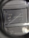
| Part Number | MAX479CSD |
|---|---|
| Manufacturer | Maxim Integrated |
| Description | IC OPAMP GP 85KHZ 14SOIC |
| Datasheet | |
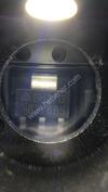
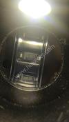
| Package | 14-SOIC (0.154", 3.90mm Width) |
| ECAD |
|
| In Stock | 4,944 piece(s) |
| Unit Price | Request a Quote |
| Lead Time | Can Ship Immediately |
| Estimated Delivery Time | Apr 27 - May 2 (Choose Expedited Shipping) |
| Request for Quotation |
|
| Payment Methods | |
| Delivery Services |
Part Number # MAX479CSD (Linear - Amplifiers - Instrumentation, OP Amps, Buffer Amps) is manufactured by Maxim Integrated and distributed by Heisener. Being one of the leading electronics distributors, we carry many kinds of electronic components from some of the world’s top class manufacturers. Their quality is guaranteed by its stringent quality control to meet all required standards.
For MAX479CSD specifications/configurations, quotation, lead time, payment terms of further enquiries please have no hesitation to contact us. To process your RFQ, please add MAX479CSD with quantity into BOM. Heisener.com does NOT require any registration to request a quote of MAX479CSD.
| Manufacturer | Maxim Integrated |
| Category | Integrated Circuits (ICs) - Linear - Amplifiers - Instrumentation, OP Amps, Buffer Amps |
| Package | 14-SOIC (0.154", 3.90mm Width) |
| ECAD |
|
| Series | - |
| Amplifier Type | General Purpose |
| Number of Circuits | 4 |
| Output Type | - |
| Slew Rate | 0.04 V/µs |
| Gain Bandwidth Product | 85kHz |
| -3db Bandwidth | - |
| Current - Input Bias | 3nA |
| Voltage - Input Offset | 100µV |
| Current - Supply | 17µA |
| Current - Output / Channel | - |
| Voltage - Supply, Single/Dual (±) | 3 V ~ 30 V, ±1.5 V ~ 15 V |
| Operating Temperature | 0°C ~ 70°C |
| Mounting Type | Surface Mount |
| Package / Case | 14-SOIC (0.154", 3.90mm Width) |
| Supplier Device Package | 14-SOIC |
Freder*****ugherty
April 6, 2023
Salva*****illis
March 20, 2023
Chai*****thews
March 20, 2023


|
2220Y2500153JXT | Knowles Syfer, CAP CER 2220, -, - | View |

|
SGD06N60BUMA1 | Infineon Technologies, IGBT 600V 12A 68W TO252-3, TO-252-3, DPak (2 Leads + Tab), SC-63, - | View |

|
LV8729V-MPB-H | ON Semiconductor, IC MOTOR DRIVER PAR SSOP44K, 44-LSSOP (0.220", 5.60mm Width) Exposed Pad, - | View |
 
|
AD7548JN | Analog Devices Inc., IC DAC 12BIT LC2MOS 20-DIP, 20-DIP (0.300", 7.62mm), - | View |

|
AR0805FR-07680KL | Yageo, RES SMD 680K OHM 1% 1/8W 0805, 0805 (2012 Metric), - | View |
|
|
TS04710A0000G | Amphenol Anytek, TERM BLOCK PLUG 4POS 90DEG 5MM, -, - | View |
|
|
1-1437540-2 | TE Connectivity AMP Connectors, CONN IC DIP SOCKET 36POS TIN, -, - | View |
|
|
FW-17-03-L-D-085-150-P | Samtec Inc., .050'' BOARD SPACERS, -, - | View |
|
|
CA00COMME14S-6PB | ITT Cannon, LLC, CONN RCPT 6POS WALL MNT PIN, -, - | View |
|
|
88-628742-35P | Amphenol Aerospace Operations, TVP00RW-11-35P W/ PC & CLN, -, - | View |
|
|
EMM06DTBT-S664 | Sullins Connector Solutions, CONN EDGE DUAL FMALE 12POS 0.156, -, - | View |

|
ISL8012IRZ-T7A | Renesas Electronics America, IC REG BUCK ADJ 2A SYNC 10DFN, 10-VFDFN Exposed Pad, - | View |

We guarantee 100% customer satisfaction.
Our experienced sales team and tech support team back our services to satisfy all our customers.

We provide 90 days warranty.
If the items you received were not in perfect quality, we would be responsible for your refund or replacement, but the items must be returned in their original condition.
| Part Number | Manufacturer | Description | Stock |
MAX479CSD |
Maxim Integrated Products | 88 |
| Part Number | Manufacturer | Description | Stock |
MAX479CSD |
Maxim Integrated Products |
IC OPAMP GP 85KHZ 14SOIC |
0 |
| Part Number | Manufacturer | Description | Stock |
MAX479CSD D# MAX479CSD-ND |
Maxim Integrated Products |
IC OPAMP GP 4 CIRCUIT 14SOIC |
0 |
| Part Number | Manufacturer | Description | Stock |
MAX479CSD+T D# MAX479CSD+T |
Maxim Integrated Products |
Industry Leading ISO:9001/AS9120A Stocking Distributor of Obsolete & Hard to Find IC's/Semi's, Specializing in Altera/Xilinx. In-House Counterfeit Detection Lab. In Business 20 Years. Free Shipping on Orders Over $250. Buy American, Buy Direct |
1919 |
MAX479CSD D# MAX479CSD |
Maxim Integrated Products |
Industry Leading ISO:9001/AS9120A Stocking Distributor of Obsolete & Hard to Find IC's/Semi's, Specializing in Altera/Xilinx. In-House Counterfeit Detection Lab. In Business 20 Years. Free Shipping on Orders Over $250. Buy American, Buy Direct |
3378 |
| Part Number | Manufacturer | Description | Stock |
MAX479CSDT |
Maxim Integrated Products |
OEM/CM QUOTES ONLY | NO BROKERS |
7952 |
MAX479CSDSMD |
N/A |
OEM/CM QUOTES ONLY | NO BROKERS |
1 |
MAX479CSD |
OEM/CM QUOTES ONLY | NO BROKERS |
4011 |
| Part Number | Manufacturer | Description | Stock |
MAX479CSDTSOIC14 |
Maxim Integrated Products |
OEM/CM ONLY |
239 |
MAX479CSDSO14 |
Maxim Integrated Products |
OEM/CM ONLY |
377 |
MAX479CSD |
Maxim Integrated Products |
OEM/CM ONLY |
146 |
MAX479CSDWCSD |
Maxim Integrated Products |
OEM/CM ONLY |
238 |
MAX479CSDT |
Maxim Integrated Products |
OEM/CM ONLY |
853 |
| Part Number | Manufacturer | Description | Stock |
MAX479CSD D# NS-MAX479CSD |
Maxim Integrated Products |
OEM/CM ONLY |
8269 |
| Part Number | Manufacturer | Description | Stock |
MAX479CSD |
Maxim Integrated Products |
Operational Amplifier, Quad AMP, Bipolar, 14 Pin, Plastic, SOP |
70 |
| Part Number | Manufacturer | Description | Stock |
MAX479CSDT |
Dallas Semiconductor |
OEM/CM ONLY |
6866 |
MAX479CSD+ |
Maxim Integrated Products |
OEM/CM ONLY |
388 |
| Part Number | Manufacturer | Description | Stock |
MAX479CSD |
Maxim Integrated Products |
RFQ |
1647 |
MAX479CSD+ |
Maxim Integrated Products |
RFQ |
3290 |
MAX479CSD+T |
Maxim Integrated Products |
RFQ |
7528 |
Heisener's commitment to quality has shaped our processes for sourcing, testing, shipping, and every step in between. This foundation underlies each component we sell.

Do you have any question about MAX479CSD?
+86-755-83210135-818


Scan to view this page