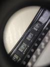
Part Number | MAX6825SUK+T |
---|---|
Manufacturer | Maxim Integrated |
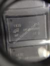
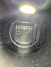
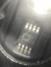
Description | IC MPU SUPERVISOR SOT23-5 |
Datasheet | MAX6825SUK+T Datasheet |
Package | SC-74A, SOT-753 |
In Stock | 1,288 piece(s) |
Unit Price | $ 4.8700 * |
Lead Time | Can Ship Immediately |
Estimated Delivery Time | Jan 24 - Jan 29 (Choose Expedited Shipping) |
Request for Quotation |
|
Part Number # MAX6825SUK+T (PMIC - Supervisors) is manufactured by Maxim Integrated and distributed by Heisener. Being one of the leading electronics distributors, we carry many kinds of electronic components from some of the world’s top class manufacturers. Their quality is guaranteed by its stringent quality control to meet all required standards.
For MAX6825SUK+T specifications/configurations, quotation, lead time, payment terms of further enquiries please have no hesitation to contact us. To process your RFQ, please add MAX6825SUK+T with quantity into BOM. Heisener.com does NOT require any registration to request a quote of MAX6825SUK+T.
Manufacturer | Maxim Integrated |
Category | Integrated Circuits (ICs) - PMIC - Supervisors |
Datasheet | MAX6825SUK+TDatasheet |
Package | SC-74A, SOT-753 |
Series | - |
Type | Simple Reset/Power-On Reset |
Number of Voltages Monitored | 1 |
Output | Push-Pull, Totem Pole |
Reset | Active High/Active Low |
Reset Timeout | 140 ms Minimum |
Voltage - Threshold | 2.93V |
Operating Temperature | -40°C ~ 125°C (TA) |
Mounting Type | Surface Mount |
Package / Case | SC-74A, SOT-753 |
Supplier Device Package | SOT-23-5 |
● Set-Top Boxes ● Computers and Con- trollers ● Embedded Controllers ● Intelligent Instruments ● Critical µP Monitoring ● Portable/Battery- Powered Equipment General Description The MAX6821–MAX6825 are low-voltage microproces- sor (µP) supervisory circuits that combine voltage mon- itoring, watchdog timer, and manual reset input func- tions in a 5-pin SOT23 package. Microprocessor super- visory circuits significantly improve system reliability and accuracy compared to separate ICs or discrete compo- nents. These devices assert a reset signal whenever the monitored voltage drops below its preset threshold, keep- ing it asserted for a minimum timeout period after VCC rises above the threshold. In addition, a watchdog timer monitors against code execution errors. A debounced manual reset is also available. The MAX6821–MAX6825 monitor voltag- es from +1.8V to +5.0V. These outputs are guaranteed to be in the correct state for VCC down to +1.0V. Nine preprogrammed reset threshold voltages are available (see the Threshold Suffix Guide). The MAX6821, MAX6822, and MAX6823 all have a manual reset input and a watchdog timer. The MAX6821 has push-pull RESET, the MAX6822 has open-drain RESET, and the MAX6823 has push-pull RESET. The MAX6824 has a watchdog timer and both push-pull RESET and push-pull RESET. The MAX6825 has a manual reset input and both push-pull RESET and push-pull RESET. The Selector Guide explains the functions offered in this series of parts. Features ● Monitors +1.8V, +2.5V, +3.0V, +3.3V, +5.0V Supplies ● 140ms (min) Reset Timeout Delay ● 1.6s Watchdog Timeout Period (MAX6821/MAX6822/ MAX6823/MAX6824) ● Manual Reset Input (MAX6821/MAX6822/MAX6823/ MAX6825) ● Three Reset Output Options Push-Pull RESET Push-Pull RESET Open-Drain RESET ● Guaranteed Reset Valid to VCC = +1.0V ● Immune to Short Negative VCC Transients ● No External Components ● Small 5-Pin SOT23 Packages Applications 19-1868; Rev 3; 7/14 Note: Bold indicates standard versions. Samples are typically available for standard versions only. All parts require a 2.5k minimum order increment. Contact factory for availability. *Insert the desired suffix letter (from the table below) into the blank to complete the part number Devices are available in both leaded and lead(Pb)-free packag- ing.Specify lead-free by replacing “-T” with “+T” when ordering. SUFFIX RESETTHRESHOLD (V) L 4.63 M 4.38 T 3.08 S 2.93 R 2.63 Z 2.32 Y 2.19 W 1.67 V 1.58 PART* TEMP RANGE PIN-PACKAGE MAX6821_UK-T -40°C to +125°C 5 SOT23-5 MAX6822_UK-T -40°C to +125°C 5 SOT23-5 MAX6823_UK-T -40°C to +125°C 5 SOT23-5 MAX6824_UK-T -40°C to +125°C 5 SOT23-5 MAX6825_UK-T -40°C to +125°C 5 SOT23-5 GND WDIMR 1 5 VCCRESET(RESET) (RESET) MAX6821 ONLY MAX6821 MAX6822 MAX6823 SOT23-5 TOP VIEW 2 3 4 MAX6821/MAX6825 Low-Voltage SOT23 µP Supervisors with Manual Reset and Watchdog Timer Selector Guide appears at end of data sheet. Threshold Suffix Guide Ordering Information Typical Operating Circuit appears at end of data sheet. Pin Configurations continued at end of data sheet. Pin Configurations
VCC to GND .........................................................-0.3V to +6.0V Open-Drain RESET ..............................................-0.3V to +6.0V Push-Pull RESET, RESET, MR, WDI ....... -0.3V to (VCC + 0.3V) Input Current (VCC) ............................................................20mA Output Current (RESET, RESET) ......................................20mA Continuous Power Dissipation (TA = +70°C) 5-Pin SOT23 (derate 7.1mW/°C above +70°C) ..........571mW Operating Temperature Range ......................... -40°C to +125°C Junction Temperature ......................................................+150°C Storage Temperature Range ............................ -65°C to +150°C Lead Temperature (soldering, 10s) .................................+300°C (VCC = +4.5V to +5.5V for MAX682_L/M, VCC = +2.7V to +3.6V for MAX682_T/S/R, VCC = +2.1V to +2.75V for MAX682_Z/Y, VCC = +1.53V to +2.0V for MAX682_W/V, TA = -40°C to +125°C, unless otherwise specified. Typical values are at TA = +25°C.) (Note 1) PARAMETER SYMBOL CONDITIONS MIN TYP MAX UNITS Operating Voltage Range VCC TA = 0°C to +85°C 1.0 5.5 V TA = -40°C to +125°C 1.2 5.5 VCC Supply Current (MR and WDI Unconnected) ICC VCC = +5.5V, no load TA = -40°C to +85°C 10 20 µA TA = -40°C to +125°C 30 VCC = +3.6V, no load TA = -40°C to +85°C 7 16 TA = -40°C to +125°C 25 VCC = +3.6V, no load (MAX6825 only) TA = -40°C to +85°C 5 12 TA = -40°C to +125°C 20 VCC Reset Threshold (VCC Falling) VTH MAX682_L TA = -40°C to +85°C 4.50 4.63 4.75 V TA = -40°C to +125°C 4.47 4.63 4.78 MAX682_M TA = -40°C to +85°C 4.25 4.38 4.50 TA = -40°C to +125°C 4.22 4.38 4.53 MAX682_T TA = -40°C to +85°C 3.00 3.08 3.15 TA = -40°C to +125°C 2.97 3.08 3.17 MAX682_S TA = -40°C to +85°C 2.85 2.93 3.00 TA = -40°C to +125°C 2.83 2.93 3.02 MAX682_R TA = -40°C to +85°C 2.55 2.63 2.70 TA = -40°C to +125°C 2.53 2.63 2.72 MAX682_Z TA = -40°C to +85°C 2.25 2.32 2.38 TA = -40°C to +125°C 2.24 2.32 2.40 MAX682_Y TA = -40°C to +85°C 2.12 2.19 2.25 TA = -40°C to +125°C 2.11 2.19 2.27 MAX682_W TA = -40°C to +85°C 1.62 1.67 1.71 TA = -40°C to +125°C 1.61 1.67 1.72 MAX682_V TA = -40°C to +85°C 1.52 1.58 1.62 Reset Threshold Temperature Coefficient 60 ppm/°C Reset Threshold Hysteresis 2 × VTH mV VCC to Reset Output Delay tRD VCC = VTH to (VTH - 100mV) 20 µs www.maximintegrated.com Maxim Integrated │ 2 MAX6821/MAX6825 Low-Voltage SOT23 µP Supervisors with Manual Reset and Watchdog Timer Electrical Characteristics Stresses beyond those listed under “Absolute Maximum Ratings” may cause permanent damage to the device. These are stress ratings only, and functional operation of the device at these or any other conditions beyond those indicated in the operational sections of the specifications is not implied. Exposure to absolute maximum rating conditions for extended periods may affect device reliability. Absolute Maximum Ratings
Note 1: Over-temperature limits are guaranteed by design and not production tested. Devices tested at TA = +25°C. Note 2: Guaranteed by design and not production tested. (VCC = +4.5V to +5.5V for MAX682_L/M, VCC = +2.7V to +3.6V for MAX682_T/S/R, VCC = +2.1V to +2.75V for MAX682_Z/Y, VCC = +1.53V to +2.0V for MAX682_W/V, TA = -40°C to +125°C, unless otherwise specified. Typical values are at TA = +25°C.) (Note 1) PARAMETER SYMBOL CONDITIONS MIN TYP MAX UNITS Reset Timeout Period tRP TA = -40°C to +85°C 140 200 280 msTA = -40°C to +125°C 100 320 RESET Output LOW (Push-Pull or Open-Drain) VOL VCC ≥ 1.0V, ISINK = 50µA, reset asserted, TA = 0°C to +85°C 0.3 VVCC ≥ 1.2V, ISINK = 100µA, reset asserted 0.3 VCC ≥ 2.55V, ISINK = 1.2mA, reset asserted 0.3 VCC ≥ 4.25V, ISINK = 3.2mA, reset asserted 0.4 RESET Output HIGH (Push-Pull Only) VOH VCC ≥ 1.8V, ISOURCE = 200µA, reset not asserted 0.8 × VCC VVCC ≥ 3.15V, ISOURCE = 500µA, reset notasserted 0.8 × VCC VCC ≥ 4.75V, ISOURCE = 800µA, reset not asserted 0.8 × VCC Open-Drain RESET Output Leakage Current (Note 1) ILKG VCC > VTH, RESET not asserted 1.0 µA RESET Output HIGH (Push-Pull Only) VOH VCC ≥ 1.0V, ISOURCE = 1µA, reset asserted, TA = 0°C to +85°C 0.8 × VCC VVCC ≥ 1.50V, ISOURCE = 100µA, reset asserted 0.8 × VCC VCC ≥ 2.55V, ISOURCE = 500µA, reset asserted 0.8 × VCC VCC ≥ 4.25V, ISOURCE = 800µA, reset asserted 0.8 × VCC RESET Output LOW (Push-Pull Only) VOL VCC ≥ 1.8V, ISINK = 500µA, reset not asserted 0.3 VVCC ≥ 3.15V, ISINK = 1.2mA, reset not asserted 0.3 VCC ≥ 4.75V, ISINK = 3.2mA, reset not asserted 0.4 MANUAL RESET INPUT (MAX6821/MAX6822/MAX6823/MAX6825) MR Input Voltage VIL 0.3 × VCC V VIH 0.7 × VCC MR Minimum Input Pulse 1 µs MR Glitch Rejection 100 ns MR to Reset Delay 200 ns MR Pullup Resistance 25 50 75 kΩ WATCHDOG INPUT (MAX6821/MAX6822/MAX6823/MAX6824) Watchdog Timeout Period tWD TA = -40°C to +85°C 1.12 1.60 2.40 s TA = -40°C to +125°C 0.80 2.60 WDI Pulse Width (Note 2) tWDI 50 ns WDI Input Voltage VIL 0.3 × VCC V VIH 0.7 × VCC WDI Input Current IWDI WDI = VCC, time average 120 160 µA WDI = 0, time average -20 -15 www.maximintegrated.com Maxim Integrated │ 3 MAX6821/MAX6825 Low-Voltage SOT23 µP Supervisors with Manual Reset and Watchdog Timer Electrical Characteristics (continued)
(TA = +25°C, unless otherwise noted.) 2.74 2.78 2.76 2.82 2.80 2.84 2.86 2.90 2.88 2.92 0 0.1 0.2 0.3 0.4 0.5 0.6 0.7 0.8 0.9 1.0 VOLTAGE OUTPUT HIGH vs. SOURCE CURRENT M AX 68 21 to c0 8 ISOURCE (mA) V O UT (V ) VCC = +2.9V 0 0.10 0.05 0.20 0.15 0.30 0.25 0.35 0 2 31 4 5 6 7 VOLTAGE OUTPUT LOW vs. SINK CURRENT M AX 68 21 to c0 7 ISINK (mA) V O UT (V ) VCC = +2.9V 0 60 40 20 80 100 120 0 806020 40 100 120 140 160 180 200 MAXIMUM VCC TRANSIENT DURATION vs. RESET THRESHOLD OVERDRIVE M AX 68 21 to c0 6 RESET THRESHOLD OVERDRIVE (mV), VTH - VCC TR AN SI EN T DU RA TI ON (µ s) RESET OCCURS ABOVE CURVE 0.94 0.96 1.00 0.98 1.04 1.02 1.06 -40 0 20-20 40 60 80 100 120 NORMALIZED RESET THRESHOLD DELAY vs. TEMPERATURE M AX 68 21 to c0 5 TEMPERATURE (°C) RE SE T TH RE SH OL D (V ) 1.0 1.2 1.1 1.4 1.3 1.6 1.5 1.7 1.9 1.8 2.0 -40 0 20 40-20 60 80 100 120 WATCHDOG TIMEOUT PERIOD vs. TEMPERATURE M AX 68 21 to c0 4 TEMPERATURE (°C) W AT CH DO G TI ME OU T PE RI OD (s ) 0 10 5 20 15 30 25 35 -40 0 20-20 40 60 80 100 120 VCC TO RESET OUTPUT DELAY vs. TEMPERATURE M AX 68 21 to c0 3 TEMPERATURE (°C) PR OP AG AT IO N DE LA Y (µ s) VCC FALLING, VCC = VTH - 100mV TEMPERATURE (°C) 150 170 160 190 180 210 200 220 240 230 250 -40 0 20 40-20 60 80 100 120 RESET TIMEOUT PERIOD vs. TEMPERATURE M AX 68 21 to c0 2 RE SE T TI ME OU T PE RI OD (m s) 3 5 4 7 6 9 8 10 12 11 13 -40 0 20 40-20 60 80 100 120 SUPPLY CURRENT vs. TEMPERATURE M AX 68 21 to c0 1 TEMPERATURE (°C) SU PP LY C UR RE NT (µ A) VCC = +5V, L VERSION VCC = +3.3V, S VERSION VCC = +1.8V, V VERSION Maxim Integrated │ 4www.maximintegrated.com MAX6821/MAX6825 Low-Voltage SOT23 µP Supervisors with Manual Reset and Watchdog Timer Typical Operating Characteristics
Detailed Description RESET/RESET Output A µP’s reset input starts the µP in a known state. The MAX6821–MAX6825 µP supervisory circuits assert a reset to prevent code-execution errors during power-up, power-down, and brownout conditions. Whenever VCC falls below the reset threshold, the reset output asserts low for RESET and high for RESET. Once VCC exceeds the reset threshold, an internal timer keeps the reset out- put asserted for the specified reset timeout period (tRP); after this interval, reset output returns to its original state (see Figure 2). Manual Reset Input Many µP-based products require manual reset capabili- ty, allowing the operator, a test technician, or external logic circuitry to initiate a reset. On the MAX6821/ MAX6822/MAX6823/MAX6825, a logic low on MR asserts a reset. Reset remains asserted while MR is low, and for the timeout period (140ms min) after it returns high. MR has an internal 50kΩ pullup resistor, so it can be left open if not used. This input can be dri- ven with CMOS logic levels or with open-drain/collector outputs. Connect a normally open momentary switch from MR to GND to create a manual reset function; external debounce circuitry is not required. If MR is dri- ven from long cables or the device is used in a noisy environment, connect a 0.1µF capacitor from MR to GND to provide additional noise immunity. Watchdog Input In the MAX6821–MAX6824, the watchdog circuit moni- tors the µP’s activity. If the µP does not toggle (low to high or high to low) the watchdog input (WDI) within the watchdog timeout period (1.6s nominal), reset asserts for the reset timoeout period. The internal 1.6s timer can be cleared by either a reset pulse or by toggling WDI. The WDI can detect pulses as short as 50ns. While reset is asserted, the timer remains cleared and does not count. As soon as reset is released, the timer starts counting (see Figure 3). PIN NUMBERS PIN NAME FUNCTIONMAX6821 MAX6822 MAX6823 MAX6824 MAX6825 1 1 1 1 RESET Active-Low Open-Drain or Push-Pull Reset Output. RESET changes from high to low when the VCC input drops below the selected reset threshold, MR is pulled low, or the watchdog triggers a reset. RESET remains low for the reset timeout period after VCC exceeds the device reset threshold, MR goes low to high, or the watchdog triggers a reset. 1 3 3 RESET Active-High Push-Pull Reset Output. RESET changes from low to high when the VCC input drops below the selected reset threshold, MR is pulled low, or the watchdog triggers a reset. RESET remains high for the reset timeout period after VCC exceeds the device reset threshold, MR goes low to high, or the watchdog triggers a reset. 2 2 2 2 2 GND Ground 3 3 3 4 MR Active-Low Manual Reset Input. Internal 50kΩ pullup to VCC. Pull low to force a reset. Reset remains active as long as MR is low and for the reset timeout period after MR goes high. Leave unconnected or connect to VCC if unused. 4 4 4 4 WDI Watchdog Input. If WDI remains high or low for longer than the watchdog timeout period, the internal watchdog timer runs out and a reset is triggered for the reset timeout period. The internal watchdog timer clears whenever reset is asserted, the manual reset is asserted, or WDI sees a rising or falling edge. If WDI is left unconnected or is connected to a three-stated buffer output, the watchdog feature is disabled. 5 5 5 5 5 VCC Supply Voltage and Input for Reset Threshold Monitor www.maximintegrated.com Maxim Integrated │ 5 MAX6821/MAX6825 Low-Voltage SOT23 µP Supervisors with Manual Reset and Watchdog Timer Pin Description
Disable the watchdog function by leaving WDI uncon- nected or by three-stating the driver connected to WDI. The watchdog input is internally driven low during the first 7/8 of the watchdog timeout period and high for the last 1/8 of the watchdog timeout period. When WDI is left unconnected, this internal driver clears the 1.6s timer every 1.4s. When WDI is three-stated or unconnected, the maximum allowable leakage current is 10µA and the maximum allowable load capacitance is 200pF. Applications Information Watchdog Input Current The MAX6821/MAX6822/MAX6823/MAX6824 WDI inputs are internally driven through a buffer and series resistor from the watchdog timer (Figure 1). When WDI is left unconnected, the watchdog timer is serviced within the watchdog timeout period by a low-high-low pulse from the counter chain. For minimum watchdog input current (minimum overall power consumption), leave WDI low for the majority of the watchdog timeout period, pulsing it low- high-low once within the first 7/8 of the watchdog timeout period to reset the watchdog timer. If WDI is externally driven high for the majority of the timeout period, up to 160µA can flow into WDI. Interfacing to µPs with Bidirectional Reset Pins Since the RESET output on the MAX6822 is open drain, it interfaces easily with µPs that have bidirectional reset pins, such as the Motorola 68HC11. Connecting the µP supervisor’s RESET output directly to the microcon- troller’s RESET pin with a single pullup resistor allows either device to assert reset (see Figure 4). Negative-Going VCC Transients These supervisors are relatively immune to short-dura- tion, negative-going VCC transients (glitches), which usually do not require the entire system to shut down. Figure 2. Reset Timing Diagram Figure 1. Functional Diagram VCC 1V1V tRD VTH VTH tRDRESET GND RESET tRP tRP MAX6821– MAX6825 VCC VCC WDI (MAX6821–MAX6824) 1.26V GND RESET (MAX6821/MAX6824/ MAX6825) RESET (MAX6822–MAX6825) MR (MAX6821–MAX6823, MAX6825) RESET GENERATOR WATCHDOG TIMER WATCHDOG TRANSITION DETECTOR www.maximintegrated.com Maxim Integrated │ 6 MAX6821/MAX6825 Low-Voltage SOT23 µP Supervisors with Manual Reset and Watchdog Timer
Resets are issued to the µP during power-up, pow- er-down, and brownout conditions. The Typical Operating Characteristics show a graph of the MAX6821–MAX6825’s Maximum VCC Transient Duration vs. Reset Threshold Overdrive, for which reset pulses are not generated. The graph was produced using negative-going VCC pulses, starting at the standard monitored voltage and ending below the reset threshold by the magnitude indicated (reset threshold overdrive). The graph shows the max- imum pulse width that a negative-going VCC transient can typically have without triggering a reset pulse. As the amplitude of the transient increases (i.e., goes farther below the reset threshold), the maximum allowable pulse width decreases. Typically, a VCC transient that goes 100mV below the reset threshold and lasts for 20µs or less will not trigger a reset pulse. Watchdog Software Considerations One way to help the watchdog timer monitor software execution more closely is to set and reset the watchdog input at different points in the program, rather than pulsing the watchdog input high-low-high or low-high-low. This technique avoids a stuck loop, in which the watchdog timer would continue to be reset inside the loop, keeping the watchdog from timing out. Figure 5 shows an example of a flow diagram where the I/O driving the watchdog input is set high at the begin- ning of the program, set low at the beginning of every subroutine or loop, then set high again when the program returns to the beginning. If the program should hang in any subroutine, the problem would quickly be corrected, since the I/O is continually set low and the watchdog timer is allowed to time out, causing a reset or interrupt to be issued. As described in the Watchdog Input Current section, this scheme results in higher time average WDI input current than does leaving WDI low for the majority of the timeout period and periodically pulsing it low-high-low. Figure 5. Watchdog Flow Diagram Figure 4. Interfacing open-Drain RESET to µPs with Bidirectional Reset I/O Figure 3. Watchdog Timing Relationship MAX6823 µP VCC VCC VCC GNDMANUAL RESET RESET I/O RESET MR WDI START SET WDI HIGH PROGRAM CODE SUBROUTINE OR PROGRAM LOOP SET WDI LOW RETURN MAX6822 RESET GENERATOR GND GND VCC VCC RESET RESET µP VCC tWD tRP tRP tRST WDI RESET* *RESET IS THE INVERSE OF RESET. www.maximintegrated.com Maxim Integrated │ 7 MAX6821/MAX6825 Low-Voltage SOT23 µP Supervisors with Manual Reset and Watchdog Timer Typical Operating Circuit
FUNCTION ACTIVE-LOW RESET ACTIVE-HIGH RESET OPEN-DRAIN RESET WATCHDOG INPUT MANUAL RESET INPUT MAX6821 — ✔ — ✔ ✔ MAX6822 — — ✔ ✔ ✔ MAX6823 ✔ — — ✔ ✔ MAX6824 ✔ ✔ — ✔ — MAX6825 ✔ ✔ — — ✔ PACKAGE TYPE PACKAGE CODE OUTLINE NO. LAND PATTERN NO. 5 SOT23 U5-1 21-0057 — GND WDIRESET 1 5 VCCRESET MAX6824 SOT23-5 TOP VIEW 2 3 4 GND MRRESET 1 5 VCCRESET MAX6825 SOT23-5 2 3 4 www.maximintegrated.com Maxim Integrated │ 8 MAX6821/MAX6825 Low-Voltage SOT23 µP Supervisors with Manual Reset and Watchdog Timer Package Information For the latest package outline information and land patterns (footprints), go to www.maximintegrated.com/packages. Note that a “+”, “#”, or “-” in the package code indicates RoHS status only. Package drawings may show a different suffix character, but the drawing pertains to the package regardless of RoHS status. Chip Information TRANSISTOR COUNT: 750 PROCESS: BiCMOS Pin Configurations (continued) Selector Guide
Lar*****Karan
December 19, 2020
Chris*****Peralta
December 19, 2020
Maxw*****Levy
December 17, 2020
Grac***** Uppal
December 14, 2020
Artu*****alsh
December 12, 2020
Abdul*****arding
December 8, 2020
Kayl*****owers
December 5, 2020
Ari*****Dutt
November 26, 2020
We guarantee 100% customer satisfaction.
Our experienced sales team and tech support team back our services to satisfy all our customers.
We provide 90 days warranty.
If the items you received were not in perfect quality, we would be responsible for your refund or replacement, but the items must be returned in their original condition.
Payment Methods | |
Delivery Services |
Heisener's commitment to quality has shaped our processes for sourcing, testing, shipping, and every step in between. This foundation underlies each component we sell.