| Part Number | MC34844AEPR2 |
|---|---|
| Manufacturer | NXP |
| Description | IC LED DRVR RGLTR DIM 80MA 32QFN |
| Datasheet | |
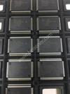
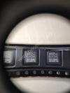
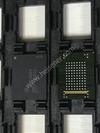
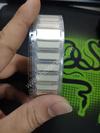
| Package | 32-VFQFN Exposed Pad |
| ECAD |
|
| In Stock | 7,020 piece(s) |
| Unit Price | $ 4.5395 * |
| Lead Time | Can Ship Immediately |
| Estimated Delivery Time | Apr 28 - May 3 (Choose Expedited Shipping) |
| Request for Quotation |
|
| Payment Methods | |
| Delivery Services |
Part Number # MC34844AEPR2 (PMIC - LED Drivers) is manufactured by NXP and distributed by Heisener. Being one of the leading electronics distributors, we carry many kinds of electronic components from some of the world’s top class manufacturers. Their quality is guaranteed by its stringent quality control to meet all required standards.
For MC34844AEPR2 specifications/configurations, quotation, lead time, payment terms of further enquiries please have no hesitation to contact us. To process your RFQ, please add MC34844AEPR2 with quantity into BOM. Heisener.com does NOT require any registration to request a quote of MC34844AEPR2.
| Manufacturer | NXP |
| Category | Integrated Circuits (ICs) - PMIC - LED Drivers |
| Package | 32-VFQFN Exposed Pad |
| ECAD |
|
| Series | - |
| Type | DC DC Regulator |
| Topology | Step-Up (Boost) |
| Internal Switch(s) | Yes |
| Number of Outputs | 10 |
| Voltage - Supply (Min) | 7V |
| Voltage - Supply (Max) | 28V |
| Voltage - Output | 8 V ~ 60 V |
| Current - Output / Channel | 80mA |
| Frequency | - |
| Dimming | Analog, PWM |
| Applications | Backlight |
| Operating Temperature | -40°C ~ 105°C (TA) |
| Mounting Type | Surface Mount |
| Package / Case | 32-VFQFN Exposed Pad |
| Supplier Device Package | 32-QFN Exposed Pad (5x5) |
Jorge*****hinson
April 5, 2023
Jocel*****nkaran
March 31, 2023
Zecha*****Ravel
March 30, 2023
Cai*****unda
March 22, 2023
Dari*****hokshi
March 21, 2023
Cairo*****simhan
March 6, 2023
Rosal*****bster
February 23, 2023
Zar*****Costa
February 20, 2023


|
SGR-8002DC-STM | EPSON, OSC PROG TTL 5V STBY 100PPM TH, 8-DIP, 4 Leads (Half Size), - | View |

|
SIT9120AI-2D2-25S100.000000Y | SiTIME, -40 TO 85C, 7050, 25PPM, 2.5V, 1, 6-SMD, No Lead, - | View |

|
C322C562JAG5TA | KEMET, CAP CER 5600PF 250V C0G RADIAL, Radial, - | View |

|
Z8F2480PJ020SG | Zilog, IC MCU 8BIT 24KB FLASH 28DIP, 28-DIP (0.600", 15.24mm), - | View |

|
1.15108.1510000 | RAFI USA, SWITCH PUSH DPST 4A 250V, -, - | View |

|
MCR03EZPFX18R7 | Rohm Semiconductor, RES SMD 18.7 OHM 1% 1/10W 0603, 0603 (1608 Metric), - | View |

|
1788363 | Phoenix Contact, TERM BLOCK RCPT 4POS 5.08MM, -, - | View |

|
342702-7 | TE Connectivity AMP Connectors, CONN HEADER 2POS VERT TIN .156, -, - | View |

|
UTXCFL8AM | Amphenol Industrial Operations, CONN FEMALE 8AWG/10MM2, -, - | View |

|
19620005082 | HARTING, ACCES. SPECIAL CABLE CLAMP EMC M, -, - | View |
|
|
TV06DT-25-61JC | Amphenol Aerospace Operations, CONN PLUG FMALE 61POS GOLD CRIMP, -, - | View |
|
|
GBM30DTMI-S189 | Sullins Connector Solutions, CONN EDGE DUAL FMALE 60POS 0.156, -, - | View |

We guarantee 100% customer satisfaction.
Our experienced sales team and tech support team back our services to satisfy all our customers.

We provide 90 days warranty.
If the items you received were not in perfect quality, we would be responsible for your refund or replacement, but the items must be returned in their original condition.
| Part Number | Manufacturer | Description | Stock |
MC34844AEP D# E02:0323_00833246 |
NXP Semiconductors |
LED Driver 10000uA Supply Current 32-Pin QFN EP Tray RoHS: Compliant
|
0 |
MC34844AEPR2 D# V72:2272_07185878 |
NXP Semiconductors |
LED Driver 10000uA Supply Current 32-Pin QFN EP T/R RoHS: Compliant
|
0 |
| Part Number | Manufacturer | Description | Stock |
MC34844AEP/R2 D# MC34844AEPR2 |
NXP Semiconductors |
LED Driver - Tape and Reel (Alt: MC34844AEPR2) RoHS: Compliant
|
0 |
MC34844AEP D# MC34844AEP |
NXP Semiconductors |
LED DRVR 12V 32-Pin QFN EP - Bulk (Alt: MC34844AEP) RoHS: Compliant
|
0 |
| Part Number | Manufacturer | Description | Stock |
MC34844AEP D# MC34844AEP |
NXP Semiconductors |
LED DRVR 12V 32-Pin QFN EP (Alt: MC34844AEP) |
0 |
| Part Number | Manufacturer | Description | Stock |
MC34844AEP D# MC34844AEP |
NXP Semiconductors |
LED DRVR 12V 32-Pin QFN EP (Alt: MC34844AEP) |
0 |
MC34844AEP/R2 D# MC34844AEPR2 |
NXP Semiconductors |
LED Driver (Alt: MC34844AEPR2) |
0 |
| Part Number | Manufacturer | Description | Stock |
MC34844AEPR2 |
Freescale Semiconductor |
LED Backlight Driver, 10 Channel with Integrated Power Supply, QFN 32, Reel |
0 |
MC34844AEP |
Freescale Semiconductor |
LED DRIVER, BOOST, PWM, 1.3MHZ, TQFN-32, Device Topology:Boost (Step Up), No. of Outputs:10, Output Current:80mA, Output Voltage:60V, Driver Case Style:TQFN, No. of Pins:32, Input Voltage Min:7V, Input Voltage Max:28V, Packaging:Each, RoHS Compliant: Yes |
0 |
| Part Number | Manufacturer | Description | Stock |
MC34844AEPR2 D# MC34844AEPR2-ND |
NXP Semiconductors |
IC LED DRVR RGLTR DIM 80MA 32QFN |
0 |
MC34844AEP D# MC34844AEP-ND |
NXP Semiconductors |
IC LED DRVR RGLTR DIM 80MA 32QFN |
2913 |
| Part Number | Manufacturer | Description | Stock |
MC34844AEP D# MC34844AEP |
Motorola Semiconductor Products |
Industry Leading ISO:9001/AS9120A Stocking Distributor of Obsolete & Hard to Find IC's/Semi's, Specializing in Altera/Xilinx. In-House Counterfeit Detection Lab. In Business 20 Years. Free Shipping on Orders Over $250. Buy American, Buy Direct |
1456 |
| Part Number | Manufacturer | Description | Stock |
MC34844AEPR2 D# 2890080RL |
NXP Semiconductors |
LED DRIVER, BOOST, 320KHZ, TQFN-32 RoHS: Compliant
Min Qty: 1
Container: Reel
|
0 |
MC34844AEP D# 2841038 |
NXP Semiconductors |
LED DRIVER, BOOST, 1.3MHZ, TQFN RoHS: Compliant
Min Qty: 1
Container: Each
|
1426 |
| Part Number | Manufacturer | Description | Stock |
MC34844AEPR2 |
NXP Semiconductors |
RoHS: Compliant
pbFree: Yes
|
0 |
| Part Number | Manufacturer | Description | Stock |
MC34844AEPR2 |
NXP Semiconductors |
OEM/CM QUOTES ONLY | NO BROKERS |
5645 |
MC34844AEP |
Freescale Semiconductor |
OEM/CM QUOTES ONLY | NO BROKERS |
3632 |
| Part Number | Manufacturer | Description | Stock |
MC34844AEP D# 841-MC34844AEP |
NXP Semiconductors |
LED Lighting Drivers LED DRIVR W/10 CH SW RoHS: Compliant
|
2322 |
MC34844AEPR2 D# 841-MC34844AEPR2 |
NXP Semiconductors |
LED Lighting Drivers LED DRIVR W/10 CH SW RoHS: Compliant
|
8283 |
| Part Number | Manufacturer | Description | Stock |
MC34844AEP D# 49AC4003 |
NXP Semiconductors |
LED DRIVER, BOOST, 1.3MHZ, TQFN, Device Topology:Boost (Step Up), Input Voltage Min:7V, Input Voltage Max:28V, Output Voltage Max:60V, Output Current Max:81.6mA, Switching Frequency:1.3MHz, No. of Outputs:10Outputs, IC Mounting:SMD, RoHS Compliant: Yes RoHS: Compliant
Min Qty: 1
Container: Bulk
|
1426 |
MC34844AEPR2 D# 61AC0305 |
NXP Semiconductors |
LED DRIVER, BOOST, 320KHZ, TQFN-32, Device Topology:Boost, Input Voltage Min:7V, Input Voltage Max:28V, Output Voltage Max:60V, Output Current Max:80mA, Switching Frequency:320kHz, No. of Outputs:10Outputs, IC Mounting:SMD, Driver RoHS Compliant: Yes RoHS: Compliant
Min Qty: 1
Container: Cut Tape
|
4587 |
| Part Number | Manufacturer | Description | Stock |
MC34844AEP D# NS-MC34844AEP |
Freescale Semiconductor |
OEM/CM ONLY |
10163 |
MC34844AEPR2 D# NS-MC34844AEPR2 |
Freescale Semiconductor |
OEM/CM ONLY |
4853 |
| Part Number | Manufacturer | Description | Stock |
MC34844AEP |
Freescale Semiconductor |
LED DRIVER, 10-SEGMENT |
5 |
| Part Number | Manufacturer | Description | Stock |
MC34844AEP |
Freescale Semiconductor |
LED Backlight Driver, 10 Channel with Integrated Power Supply, QFN 32 RoHS: Compliant
|
806 |
| Part Number | Manufacturer | Description | Stock |
MC34844AEP |
Freescale Semiconductor |
OEM/CM ONLY |
1981 |
MC34844AEPR2 |
Freescale Semiconductor |
OEM/CM ONLY |
1508 |
| Part Number | Manufacturer | Description | Stock |
MC34844AEPR2 |
Freescale Semiconductor |
shipping today |
14496 |
| Part Number | Manufacturer | Description | Stock |
MC34844AEP D# 53200285 |
NXP Semiconductors |
LED Driver 10000uA Supply Current 32-Pin QFN EP Tray RoHS: Compliant
|
0 |
MC34844AEPR2 D# 52539617 |
NXP Semiconductors |
LED Driver 10000uA Supply Current 32-Pin QFN EP T/R RoHS: Compliant
|
0 |
| Part Number | Manufacturer | Description | Stock |
MC34844AEP |
Freescale Semiconductor |
RFQ |
6816 |
MC34844AEPR2 |
Freescale Semiconductor |
RFQ |
14841 |
| Part Number | Manufacturer | Description | Stock |
MC34844AEPR2 |
Freescale Semiconductor |
IC LED DRVR RGLTR DIM 80MA 32QFN |
870 |
MC34844AEP |
Freescale Semiconductor |
IC LED DRVR RGLTR DIM 80MA 32QFN |
870 |
| Part Number | Manufacturer | Description | Stock |
MC34844AEPR2 D# 2890080 |
NXP Semiconductors |
LED DRIVER, BOOST, 320KHZ, TQFN-32 RoHS: Compliant
Min Qty: 1
Container: Cut Tape
|
4589 |
MC34844AEP D# 2841038 |
NXP Semiconductors |
LED DRIVER, BOOST, 1.3MHZ, TQFN RoHS: Compliant
Min Qty: 1
Container: Each
|
1426 |
Heisener's commitment to quality has shaped our processes for sourcing, testing, shipping, and every step in between. This foundation underlies each component we sell.

Do you have any question about MC34844AEPR2?
+86-755-83210559 ext. 814


Scan to view this page