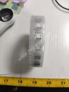
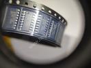
| Part Number | PAM2804AAB010 |
|---|---|
| Manufacturer | Diodes Incorporated |
| Description | IC LED DRIVER RGLTR 1A TSOT25 |
| Datasheet | |
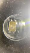
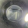
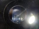
| Package | SOT-23-5 Thin, TSOT-23-5 |
| ECAD |
|
| In Stock | 1,067,088 piece(s) |
| Unit Price | $ 0.7491 * |
| Lead Time | Can Ship Immediately |
| Estimated Delivery Time | Apr 19 - Apr 24 (Choose Expedited Shipping) |
| Request for Quotation |
|
| Payment Methods | |
| Delivery Services |
Part Number # PAM2804AAB010 (PMIC - LED Drivers) is manufactured by Diodes Incorporated and distributed by Heisener. Being one of the leading electronics distributors, we carry many kinds of electronic components from some of the world’s top class manufacturers. Their quality is guaranteed by its stringent quality control to meet all required standards.
For PAM2804AAB010 specifications/configurations, quotation, lead time, payment terms of further enquiries please have no hesitation to contact us. To process your RFQ, please add PAM2804AAB010 with quantity into BOM. Heisener.com does NOT require any registration to request a quote of PAM2804AAB010.
| Manufacturer | Diodes Incorporated |
| Category | Integrated Circuits (ICs) - PMIC - LED Drivers |
| Package | SOT-23-5 Thin, TSOT-23-5 |
| ECAD |
|
| Series | - |
| Type | DC DC Regulator |
| Topology | Step-Down (Buck) |
| Internal Switch(s) | Yes |
| Number of Outputs | 1 |
| Voltage - Supply (Min) | 2.5V |
| Voltage - Supply (Max) | 6V |
| Voltage - Output | - |
| Current - Output / Channel | 1A |
| Frequency | 1.5MHz |
| Dimming | - |
| Applications | - |
| Operating Temperature | -40°C ~ 85°C (TA) |
| Mounting Type | Surface Mount |
| Package / Case | SOT-23-5 Thin, TSOT-23-5 |
| Supplier Device Package | TSOT-25 |
Kayd***** Peri
April 7, 2023
Jaxx*****ndrews
April 3, 2023
Rick*****mirez
March 31, 2023
Aly***** Soni
March 21, 2023
Kade*****lter
March 20, 2023
Ander*****llano
February 19, 2023
Devo*****gueroa
February 19, 2023


|
ECX-H22CM-16.384 | ECS Inc., OSC XO 16.3840MHZ HCMOS SMD, 6-SMD, No Lead, - | View |

|
R46KI3100JBM1M | KEMET, CAP FILM 0.1UF 20% 560VDC RADIAL, Radial, - | View |
|
|
2220J4K00222MXT | Knowles Syfer, CAP CER 2220, 2220 (5750 Metric), - | View |
|
|
1812J5K00150GCT | Knowles Syfer, CAP CER 15PF 5KV C0G/NP0 1812, 1812 (4532 Metric), - | View |

|
VJ0603D330GLPAC | Vishay Vitramon, CAP CER 33PF 250V C0G/NP0 0603, 0603 (1608 Metric), - | View |
|
|
VS-ST110S16P0PBF | Vishay Semiconductor Diodes Division, SCR 1600V 175A TO-94, TO-209AC, TO-94-4, Stud, - | View |
|
|
DSPIC33EP32GP503T-E/TL | Microchip Technology, IC MCU 16BIT 32KB FLASH 36VTLA, 36-VFTLA Exposed Pad, - | View |

|
ACASA470224702P100 | Vishay Beyschlag, RES ARRAY 4 RES 47K OHM 1206, 1206 (3216 Metric), Convex, Long Side Terminals, - | View |
 
|
ADUM1241ARZ | Analog Devices Inc., DGTL ISO 3KV 2CH GEN PURP 8SOIC, 8-SOIC (0.154", 3.90mm Width), - | View |
|
|
FTMH-120-02-H-DH-K | Samtec Inc., 1MM MICRO TERMINAL STRIPS, -, - | View |
|
|
68106-002LF | Amphenol FCI, POLARIZED M/L HSG SHROUD DBL ROW, -, - | View |
|
|
NKMJMIG | Panduit Corp, NK FIBER OPTIC ADAPTER MODULE, -, - | View |

We guarantee 100% customer satisfaction.
Our experienced sales team and tech support team back our services to satisfy all our customers.

We provide 90 days warranty.
If the items you received were not in perfect quality, we would be responsible for your refund or replacement, but the items must be returned in their original condition.
| Part Number | Manufacturer | Description | Stock |
PAM2804AAB010 D# 70437179 |
Diodes Incorporated |
Step-down LED Driver 1.5MHz 6V 1A SOT-25 RoHS: Not Compliant
|
0 |
| Part Number | Manufacturer | Description | Stock |
PAM2804AAB010 D# V72:2272_06703307 |
Zetex / Diodes Inc |
LED Driver 1 Segment 5-Pin SOT-23 T/R RoHS: Compliant
|
0 |
| Part Number | Manufacturer | Description | Stock |
PAM2804AAB010 D# PAM2804AAB010 |
Diodes Incorporated |
LED DRVR Buck 1-CH 5V 1A 5-Pin TSOT-25 T/R - Tape and Reel (Alt: PAM2804AAB010) |
0 |
| Part Number | Manufacturer | Description | Stock |
PAM2804AAB010 D# PAM2804AAB010 |
Diodes Incorporated |
LED DRVR Buck 1-CH 5V 1A 5-Pin TSOT-25 T/R (Alt: PAM2804AAB010) |
0 |
| Part Number | Manufacturer | Description | Stock |
PAM2804AAB010 D# PAM2804AAB010 |
Diodes Incorporated |
LED DRVR Buck 1-CH 5V 1A 5-Pin TSOT-25 T/R (Alt: PAM2804AAB010) |
0 |
| Part Number | Manufacturer | Description | Stock |
PAM2804AAB010 |
Diodes Incorporated |
LED Lighting Drivers 1A SD CONSTANT CRNT HI EFF LED DVR |
970 |
| Part Number | Manufacturer | Description | Stock |
PAM2804AAB010 |
Diodes Incorporated |
DC DC Regulator Step-down 2.5V 6V SOT-23-5 LED Drivers RoHS |
29550 |
| Part Number | Manufacturer | Description | Stock |
PAM2804AAB010 D# PAM2804AAB010DICT-ND |
Diodes Incorporated |
IC LED DRIVER RGLTR 1A TSOT25 |
89386 |
| Part Number | Manufacturer | Description | Stock |
PAM2804AAB010 |
Diodes Incorporated |
In stock shipping within 2days |
38025 |
| Part Number | Manufacturer | Description | Stock |
PAM2804AAB010 D# 3483111RL |
Diodes Incorporated |
LED DRIVER, BUCK, -40 TO 85DEG C RoHS: Compliant
Min Qty: 5
Container: Reel
|
0 |
| Part Number | Manufacturer | Description | Stock |
PAM2804AAB010 |
Diodes Incorporated |
OEM/CM QUOTES ONLY | NO BROKERS |
217267 |
| Part Number | Manufacturer | Description | Stock |
PAM2804AAB010 D# C71463 |
Diodes Incorporated | 29500 |
| Part Number | Manufacturer | Description | Stock |
PAM2804AAB010 |
Diodes Incorporated |
OEM/CM Immediate delivery |
210000 |
| Part Number | Manufacturer | Description | Stock |
PAM2804AAB010 D# 621-PAM2804AAB010 |
Diodes Incorporated |
LED Lighting Drivers 1A SD CONSTANT CRNT HI EFF LED DVR RoHS: Compliant
|
40171 |
| Part Number | Manufacturer | Description | Stock |
PAM2804AAB010 D# 76AH5890 |
Diodes Incorporated |
LED DRIVER, BUCK, -40 TO 85DEG C ROHS COMPLIANT: YES RoHS: Compliant
Min Qty: 5
Container: Cut Tape
|
1610 |
| Part Number | Manufacturer | Description | Stock |
PAM2804AAB010 D# NS-PAM2804AAB010 |
Diodes Incorporated |
OEM/CM ONLY |
2852 |
| Part Number | Manufacturer | Description | Stock |
PAM2804AAB010 D# 7902922 |
Zetex / Diodes Inc |
DiodesZetex PAM2804AAB010 LED Driver IC, 2.5 6 V dc 1A 5-Pin SOT-23, PK Min Qty: 10
Container: Package
|
240 |
| Part Number | Manufacturer | Description | Stock |
PAM2804AAB010 |
Diodes Incorporated |
OEM/CM ONLY |
132016 |
| Part Number | Manufacturer | Description | Stock |
PAM2804AAB010 |
Diodes Incorporated |
IN stock Immediate delivery |
209985 |
| Part Number | Manufacturer | Description | Stock |
PAM2804AAB010 |
Diodes Incorporated |
shipping today |
19796 |
| Part Number | Manufacturer | Description | Stock |
PAM2804AAB010 D# 53483076 |
Zetex / Diodes Inc |
LED Driver 1 Segment 5-Pin SOT-23 T/R RoHS: Compliant
|
0 |
| Part Number | Manufacturer | Description | Stock |
PAM2804AAB010 |
Diodes Incorporated |
IC LED DRIVER RGLTR 1A TSOT25 |
159577 |
| Part Number | Manufacturer | Description | Stock |
PAM2804AAB010 D# 3483111 |
Diodes Incorporated |
LED DRIVER, BUCK, -40 TO 85DEG C RoHS: Compliant
Min Qty: 5
Container: Cut Tape
|
1665 |
Heisener's commitment to quality has shaped our processes for sourcing, testing, shipping, and every step in between. This foundation underlies each component we sell.

Do you have any question about PAM2804AAB010?
86-755-83210559-827


Scan to view this page