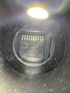
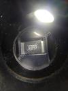
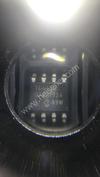
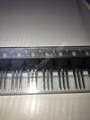
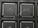
| Part Number | STA5630 |
|---|---|
| Manufacturer | STMicroelectronics |
| Description | IC RF FRONT END GPS 32VFQFPN |
| Datasheet | |
| Package | 32-VFQFN Exposed Pad |
| ECAD |
|
| In Stock | 7,164 piece(s) |
| Unit Price | Request a Quote |
| Lead Time | To be Confirmed |
| Estimated Delivery Time | Apr 22 - Apr 27 (Choose Expedited Shipping) |
| Request for Quotation |
|
| Payment Methods | |
| Delivery Services |
Part Number # STA5630 (RF Front End (LNA + PA)) is manufactured by STMicroelectronics and distributed by Heisener. Being one of the leading electronics distributors, we carry many kinds of electronic components from some of the world’s top class manufacturers. Their quality is guaranteed by its stringent quality control to meet all required standards.
For STA5630 specifications/configurations, quotation, lead time, payment terms of further enquiries please have no hesitation to contact us. To process your RFQ, please add STA5630 with quantity into BOM. Heisener.com does NOT require any registration to request a quote of STA5630.
| Manufacturer | STMicroelectronics |
| Category | RF/IF and RFID - RF Front End (LNA + PA) |
| Package | 32-VFQFN Exposed Pad |
| ECAD |
|
| Series | - |
| RF Type | GPS |
| Frequency | 1.575GHz |
| Features | - |
| Package / Case | 32-VFQFN Exposed Pad |
| Supplier Device Package | 32-VFQFPN (5x5) |
Oakl*****aniel
April 5, 2023
Cor***** Garg
April 4, 2023
Matt*****hukla
March 20, 2023
Cedr*****yers
March 16, 2023
Emberl*****ardson
February 21, 2023


|
ECQ-E12333KF | Panasonic Electronic Components, CAP FILM 0.033UF 1.25KVDC RADIAL, Radial, - | View |

|
1825Y0160472GCT | Knowles Syfer, CAP CER 4700PF 16V C0G/NP0 1825, 1825 (4564 Metric), - | View |
|
|
SA405C224MAA | AVX Corporation, CAP CER 0.22UF 50V X7R AXIAL, Axial, - | View |

|
74F646MSAX | Fairchild/ON Semiconductor, IC TXRX/REGISTER 3-ST 8B 24SSOP, 24-SSOP (0.209", 5.30mm Width), - | View |

|
CXA1820-0000-000N0UN20E5 | Cree Inc., LED ARRAY XLAMP CXA1820 WHITE, -, - | View |
|
|
HTB-38M-R | Eaton, FUSE HLDR CART 250V 16A PNL MNT, -, - | View |
|
|
0387390588 | Molex, LLC, CONN BARRIER STRIP 2CIRC 0.438", -, - | View |

|
4-102973-0-12 | TE Connectivity AMP Connectors, CONN HEADR BRKWAY .100 24POS STR, -, - | View |
|
|
DW-25-08-G-S-215 | Samtec Inc., .025" BOARD SPACERS, -, - | View |
|
|
1918538-1 | TE Connectivity AMP Connectors, CONNECTOR ASSY, LC, SM NARROW, -, - | View |
|
|
D38999/26SE6PN | Souriau, 8D 6C 6#20 PLUG, -, - | View |
|
|
DBC50H-18-32PN [V003] | TE Connectivity Deutsch Connectors, HERM RECP, -, - | View |

We guarantee 100% customer satisfaction.
Our experienced sales team and tech support team back our services to satisfy all our customers.

We provide 90 days warranty.
If the items you received were not in perfect quality, we would be responsible for your refund or replacement, but the items must be returned in their original condition.
| Part Number | Manufacturer | Description | Stock |
STA5630TR D# STA5630TR |
STMicroelectronics |
Low Power GPS RF Front-End 32-Pin VFQFPN T/R - Tape and Reel (Alt: STA5630TR) RoHS: Compliant
|
0 |
STA5630 D# STA5630 |
STMicroelectronics |
Low Power GPS RF Front-End 32-Pin VFQFPN Tray - Trays (Alt: STA5630) RoHS: Compliant
|
0 |
STA5630ATR D# STA5630ATR |
STMicroelectronics |
GPS RF Front-End 1.8V 32-Pin VFQFPN T/R - Tape and Reel (Alt: STA5630ATR) |
0 |
STA5630A D# STA5630A |
STMicroelectronics |
GPS RF Front-End 1.8V 32-Pin VFQFPN Tray - Trays (Alt: STA5630A) |
0 |
| Part Number | Manufacturer | Description | Stock |
STA5630TR D# STA5630TR |
STMicroelectronics |
Low Power GPS RF Front-End 32-Pin VFQFPN T/R (Alt: STA5630TR) |
0 |
| Part Number | Manufacturer | Description | Stock |
STA5630TR |
STMicroelectronics |
MID INFOTAINMENT - Tape and Reel |
0 |
STA5630 |
STMicroelectronics |
MID INFOTAINMENT - Tape and Reel |
0 |
| Part Number | Manufacturer | Description | Stock |
STA5630A D# STA5630A-ND |
STMicroelectronics |
GPS/GALILEO RF FRONT-END |
0 |
STA5630TR D# STA5630TR-ND |
STMicroelectronics |
IC RF FRONT END GPS 32VFQFPN |
0 |
STA5630 D# STA5630-ND |
STMicroelectronics |
IC RF FRONT END GPS 32VFQFPN |
0 |
STA5630ATR D# STA5630ATR-ND |
STMicroelectronics |
GPS/GALILEO RF FRONT-END |
0 |
| Part Number | Manufacturer | Description | Stock |
STA5630TR |
STMicroelectronics |
In stock shipping within 2days |
140 |
| Part Number | Manufacturer | Description | Stock |
STA5630ATR |
STMicroelectronics |
OEM/CM QUOTES ONLY | NO BROKERS |
833 |
STA5630A |
STMicroelectronics |
OEM/CM QUOTES ONLY | NO BROKERS |
833 |
STA5630 |
STMicroelectronics |
OEM/CM QUOTES ONLY | NO BROKERS |
774 |
STA5630TR |
STMicroelectronics |
OEM/CM QUOTES ONLY | NO BROKERS |
1855 |
| Part Number | Manufacturer | Description | Stock |
STA5630TR |
STMicroelectronics |
OEM/CM Immediate delivery |
30000 |
| Part Number | Manufacturer | Description | Stock |
STA5630ATR D# 511-STA5630ATR |
STMicroelectronics |
RF Front End Low power GPS RF front-end |
2975 |
| Part Number | Manufacturer | Description | Stock |
STA5630 D# NS-STA5630 |
STMicroelectronics |
OEM/CM ONLY |
2399 |
STA5630TR D# NS-STA5630TR |
STMicroelectronics |
OEM/CM ONLY |
4411 |
| Part Number | Manufacturer | Description | Stock |
STA5630ATR |
STMicroelectronics |
TELECOM CIRCUIT, 1-FUNC, CMOS (Also Known As: STA5630A) |
700 |
| Part Number | Manufacturer | Description | Stock |
STA5630A |
STMicroelectronics |
OEM/CM ONLY |
716 |
STA5630ATR |
STMicroelectronics |
OEM/CM ONLY |
716 |
STA5630TR |
STMicroelectronics |
OEM/CM ONLY |
1242 |
STA5630 |
STMicroelectronics |
OEM/CM ONLY |
53 |
| Part Number | Manufacturer | Description | Stock |
STA5630TR |
STMicroelectronics |
IN stock Immediate delivery |
29985 |
| Part Number | Manufacturer | Description | Stock |
STA5630TR |
STMicroelectronics |
shipping today |
45 |
Heisener's commitment to quality has shaped our processes for sourcing, testing, shipping, and every step in between. This foundation underlies each component we sell.

Do you have any question about STA5630?
+86-755-83210559 ext. 807


Scan to view this page