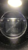
| Part Number | STM32F746BGT6 |
|---|---|
| Manufacturer | STMicroelectronics |
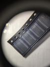
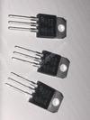
| Description | IC MCU 32BIT 1MB FLASH 208LQFP |
| Datasheet | |
| Package | 208-LQFP |
| ECAD |
|
| In Stock | 4,752 piece(s) |
| Unit Price | $ 22.8682 * |
| Lead Time | Can Ship Immediately |
| Estimated Delivery Time | Apr 26 - May 1 (Choose Expedited Shipping) |
| Request for Quotation |
|
| Payment Methods | |
| Delivery Services |
Part Number # STM32F746BGT6 (Embedded - Microcontrollers) is manufactured by STMicroelectronics and distributed by Heisener. Being one of the leading electronics distributors, we carry many kinds of electronic components from some of the world’s top class manufacturers. Their quality is guaranteed by its stringent quality control to meet all required standards.
For STM32F746BGT6 specifications/configurations, quotation, lead time, payment terms of further enquiries please have no hesitation to contact us. To process your RFQ, please add STM32F746BGT6 with quantity into BOM. Heisener.com does NOT require any registration to request a quote of STM32F746BGT6.
| Manufacturer | STMicroelectronics |
| Category | Integrated Circuits (ICs) - Embedded - Microcontrollers |
| Package | 208-LQFP |
| ECAD |
|
| Series | STM32 F7 |
| Core Processor | ARM? Cortex?-M7 |
| Core Size | 32-Bit |
| Speed | 216MHz |
| Connectivity | CAN, EBI/EMI, Ethernet, I2C, IrDA, LIN, SAI, SD, SPDIF-Rx, SPI, UART/USART, USB OTG |
| Peripherals | Brown-out Detect/Reset, DMA, I2S, LCD, POR, PWM, WDT |
| Number of I/O | 168 |
| Program Memory Size | 1MB (1M x 8) |
| Program Memory Type | FLASH |
| EEPROM Size | - |
| RAM Size | 320K x 8 |
| Voltage - Supply (Vcc/Vdd) | 1.7 V ~ 3.6 V |
| Data Converters | A/D 24x12b, D/A 2x12b |
| Oscillator Type | Internal |
| Operating Temperature | -40°C ~ 85°C (TA) |
| Mounting Type | - |
| Package / Case | 208-LQFP |
| Supplier Device Package | 208-LQFP (28x28) |
Hel***** Tata
April 4, 2023
Viva*****arma
March 23, 2023
Zav***** Dube
March 19, 2023
Mila*****alal
March 5, 2023
Elli*****Basak
February 23, 2023
Zay*****ayre
February 21, 2023
Alic*****thra
February 20, 2023


|
0805Y0160472GCR | Knowles Syfer, CAP CER 0805, 0805 (2012 Metric), STM32 F7 | View |

|
UVR1C330MDD | Nichicon, CAP ALUM 33UF 20% 16V RADIAL, Radial, Can, STM32 F7 | View |

|
MC74HC175AD | ON Semiconductor, IC D-TYPE POS TRG SNGL 16SOIC, 16-SOIC (0.154", 3.90mm Width), STM32 F7 | View |

|
AT91SAM9CN12-CFUR | Microchip Technology, IC MCU 32BIT 128KB ROM 247BGA, 247-LFBGA, STM32 F7 | View |

|
PIC16C54C-04E/SO | Microchip Technology, IC MCU 8BIT 768B OTP 18SOIC, 18-SOIC (0.295", 7.50mm Width), STM32 F7 | View |

|
CMF6023K200FHBF | Vishay Dale, RES 23.2K OHM 1W 1% AXIAL, Axial, STM32 F7 | View |

|
RNF12FTD11K0 | Stackpole Electronics Inc., RES 11K OHM 1/2W 1% AXIAL, Axial, STM32 F7 | View |

|
M20-7891646 | Harwin Inc., 16-WAY SIL HORIZ SOCKET L/FREE, -, STM32 F7 | View |
|
|
DW-33-13-F-S-890 | Samtec Inc., .025" BOARD SPACERS, -, STM32 F7 | View |
|
|
DTS20W11-5JA | TE Connectivity Deutsch Connectors, CONN RCPT 5POS FLANGE W/SKT, -, STM32 F7 | View |

|
TE40A1203Q01 | SL Power Electronics Manufacture of Condor/Ault Brands, AC/DC DESKTOP ADAPTER 12V 40W, -, STM32 F7 | View |
|
|
ZWS305/A | TDK-Lambda Americas Inc., AC/DC CONVERTER 5V 30W, -, STM32 F7 | View |

We guarantee 100% customer satisfaction.
Our experienced sales team and tech support team back our services to satisfy all our customers.

We provide 90 days warranty.
If the items you received were not in perfect quality, we would be responsible for your refund or replacement, but the items must be returned in their original condition.
| Part Number | Manufacturer | Description | Stock |
STM32F746BGT6 D# V36:1790_07447480 |
STMicroelectronics |
MCU 32-bit ARM Cortex M7 RISC 1MB Flash 1.8V/2.5V/3.3V 208-Pin LQFP Tray RoHS: Compliant
|
0 |
| Part Number | Manufacturer | Description | Stock |
STM32F746BGT6 D# STM32F746BGT6 |
STMicroelectronics |
MCU 32-Bit STM32F ARM Cortex-M7 RISC 1MB Flash 208-Pin LQFP Tray - Trays (Alt: STM32F746BGT6) |
0 |
| Part Number | Manufacturer | Description | Stock |
STM32F746BGT6 D# STM32F746BGT6 |
STMicroelectronics |
MCU 32-Bit STM32F ARM Cortex-M7 RISC 1MB Flash 208-Pin LQFP Tray (Alt: STM32F746BGT6) |
0 |
| Part Number | Manufacturer | Description | Stock |
STM32F746BGT6 D# C1S730201005107 |
STMicroelectronics |
Microcontrollers RoHS: Compliant
pbFree: Yes
Min Qty: 1
Container: Tray
|
2 |
| Part Number | Manufacturer | Description | Stock |
STM32F746BGT6 |
STMicroelectronics |
LQFP-208(28x28) ST Microelectronics RoHS |
96 |
| Part Number | Manufacturer | Description | Stock |
STM32F746BGT6 |
STMicroelectronics |
RISC Microcontroller, CMOS RoHS: Compliant
|
0 |
| Part Number | Manufacturer | Description | Stock |
STM32F746BGT6 D# 497-15815-ND |
STMicroelectronics |
IC MCU 32BIT 1MB FLASH 208LQFP |
397 |
| Part Number | Manufacturer | Description | Stock |
STM32F746BGT6 D# 2484976 |
STMicroelectronics |
MCU, 32BIT, CORTEX-M7, 216MHZ, LQFP-208 RoHS: Compliant
Min Qty: 1
Container: Each
|
0 |
| Part Number | Manufacturer | Description | Stock |
STM32F746BGT6TR |
OEM/CM QUOTES ONLY | NO BROKERS |
223 | |
STM32F746BGT6 |
STMICROELECTRONICS |
OEM/CM QUOTES ONLY | NO BROKERS |
1722 |
| Part Number | Manufacturer | Description | Stock |
STM32F746BGT6 D# C1337368 |
STMicroelectronics | 96 |
| Part Number | Manufacturer | Description | Stock |
STM32F746BGT6 |
STMicroelectronics |
OEM/CM Immediate delivery |
676 |
| Part Number | Manufacturer | Description | Stock |
STM32F746BGT6 D# 511-STM32F746BGT6 |
STMicroelectronics |
ARM Microcontrollers - MCU 16/32-BITS MICROS RoHS: Compliant
|
107 |
| Part Number | Manufacturer | Description | Stock |
STM32F746BGT6 D# 51Y5132 |
STMicroelectronics |
32 Bit Microcontroller, ART Accelerator, ARM Cortex-M7, 216 MHz, 1 MB, 320 KB, 208, LQFP RoHS Compliant: Yes RoHS: Compliant
Min Qty: 1
Container: Bulk
|
0 |
| Part Number | Manufacturer | Description | Stock |
STM32F746BGT6 D# 8820271P |
STMicroelectronics |
STMicroelectronics STM32F746BGT6, 32bit ARM Cortex M7 Microcontroller, STM32F, 216MHz, 1.024 MB Flash, OTP, 208-Pin LQFP, PU Min Qty: 1
Container: Tray
|
0 |
| Part Number | Manufacturer | Description | Stock |
STM32F746BGT6 D# ICMCU23434 |
STMicroelectronics |
Cortex M7 1024K LQFP208 85°C RoHS: Compliant
|
0 |
| Part Number | Manufacturer | Description | Stock |
STM32F746BGT6TR |
OEM/CM ONLY |
198 | |
STM32F746BGT6 |
STMicroelectronics |
OEM/CM ONLY |
1168 |
| Part Number | Manufacturer | Description | Stock |
STM32F746BGT6 |
STMicroelectronics |
IN stock Immediate delivery |
671 |
| Part Number | Manufacturer | Description | Stock |
STM32F746BGT6 D# 53314063 |
STMicroelectronics |
MCU 32-bit ARM Cortex M7 RISC 1MB Flash 1.8V/2.5V/3.3V 208-Pin LQFP Tray RoHS: Compliant
|
0 |
| Part Number | Manufacturer | Description | Stock |
STM32F746BGT6 |
STMicroelectronics |
IC MCU 32BIT 1MB FLASH 208LQFP |
300 |
| Part Number | Manufacturer | Description | Stock |
STM32F746BGT6 D# 2484976 |
STMicroelectronics |
MCU, 32BIT, CORTEX-M7, 216MHZ, LQFP-208 RoHS: Compliant
Min Qty: 1
Container: Each
|
0 |
Heisener's commitment to quality has shaped our processes for sourcing, testing, shipping, and every step in between. This foundation underlies each component we sell.

Do you have any question about STM32F746BGT6?
+86-755-83210559-827


Scan to view this page