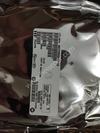
Part Number | STM8S003F3P6 |
---|---|
Manufacturer | STMicroelectronics |
Description | IC MCU 8BIT 8KB FLASH 20TSSOP |
Datasheet | STM8S003F3P6 Datasheet |
Package | 20-TSSOP (0.173", 4.40mm Width) |
In Stock | 5,820 piece(s) |
Unit Price | $ 0.8600 * |
Lead Time | Can Ship Immediately |
Estimated Delivery Time | Jan 25 - Jan 30 (Choose Expedited Shipping) |
Request for Quotation |
|
Part Number # STM8S003F3P6 (Embedded - Microcontrollers) is manufactured by STMicroelectronics and distributed by Heisener. Being one of the leading electronics distributors, we carry many kinds of electronic components from some of the world’s top class manufacturers. Their quality is guaranteed by its stringent quality control to meet all required standards.
For STM8S003F3P6 specifications/configurations, quotation, lead time, payment terms of further enquiries please have no hesitation to contact us. To process your RFQ, please add STM8S003F3P6 with quantity into BOM. Heisener.com does NOT require any registration to request a quote of STM8S003F3P6.
Manufacturer | STMicroelectronics |
Category | Integrated Circuits (ICs) - Embedded - Microcontrollers |
Datasheet | STM8S003F3P6Datasheet |
Package | 20-TSSOP (0.173", 4.40mm Width) |
Series | STM8S |
Core Processor | STM8 |
Core Size | 8-Bit |
Speed | 16MHz |
Connectivity | I2C, IrDA, LIN, SPI, UART/USART |
Peripherals | Brown-out Detect/Reset, POR, PWM, WDT |
Number of I/O | 16 |
Program Memory Size | 8KB (8K x 8) |
Program Memory Type | FLASH |
EEPROM Size | 128 x 8 |
RAM Size | 1K x 8 |
Voltage - Supply (Vcc/Vdd) | 2.95 V ~ 5.5 V |
Data Converters | A/D 5x10b |
Oscillator Type | Internal |
Operating Temperature | -40°C ~ 85°C (TA) |
Mounting Type | - |
Package / Case | 20-TSSOP (0.173", 4.40mm Width) |
Supplier Device Package | 20-TSSOP |
This is information on a product in full production. August 2018 DS7147 Rev 10 1/103 STM8S003F3 STM8S003K3 Value line, 16-MHz STM8S 8-bit MCU, 8-Kbyte Flash memory, 128-byte data EEPROM, 10-bit ADC, 3 timers, UART, SPI, I²C Datasheet - production data Features Core • 16 MHz advanced STM8 core with Harvard architecture and 3-stage pipeline • Extended instruction set Memories • Program memory: 8 Kbyte Flash memory; data retention 20 years at 55 °C after 100 cycles • RAM: 1 Kbyte • Data memory: 128 bytes true data EEPROM; endurance up to 100 k write/erase cycles Clock, reset and supply management • 2.95 V to 5.5 V operating voltage • Flexible clock control, 4 master clock sources – Low-power crystal resonator oscillator – External clock input – Internal, user-trimmable 16 MHz RC – Internal low-power 128 kHz RC • Clock security system with clock monitor • Power management – Low-power modes (wait, active-halt, halt) – Switch-off peripheral clocks individually – Permanently active, low-consumption power-on and power-down reset Interrupt management • Nested interrupt controller with 32 interrupts • Up to 27 external interrupts on 6 vectors Timers • Advanced control timer: 16-bit, 4 CAPCOM channels, 3 complementary outputs, dead-time insertion and flexible synchronization • 16-bit general purpose timer, with 3 CAPCOM channels (IC, OC or PWM) • 8-bit basic timer with 8-bit prescaler • Auto wakeup timer • Window and independent watchdog timers Communications interfaces • UART with clock output for synchronous operation, SmartCard, IrDA, LIN master mode • SPI interface up to 8 Mbit/s • I2C interface up to 400 Kbit/s Analog to digital converter (ADC) • 10-bit ADC, ± 1 LSB ADC with up to 5 multiplexed channels, scan mode and analog watchdog I/Os • Up to 28 I/Os on a 32-pin package including 21 high-sink outputs • Highly robust I/O design, immune against current injection Development support • Embedded single-wire interface module (SWIM) for fast on-chip programming and non- intrusive debugging LQFP32 7x7 mm TSSOP20 6.5x6.4 mm UFQFPN20 3x3 mm www.st.com
Contents STM8S003F3 STM8S003K3 2/103 DS7147 Rev 10 Contents 1 Introduction . . . . . . . . . . . . . . . . . . . . . . . . . . . . . . . . . . . . . . . . . . . . . . . . 9 2 Description . . . . . . . . . . . . . . . . . . . . . . . . . . . . . . . . . . . . . . . . . . . . . . . . 10 3 Block diagram . . . . . . . . . . . . . . . . . . . . . . . . . . . . . . . . . . . . . . . . . . . . . 11 4 Product overview . . . . . . . . . . . . . . . . . . . . . . . . . . . . . . . . . . . . . . . . . . 12 4.1 Central processing unit STM8 . . . . . . . . . . . . . . . . . . . . . . . . . . . . . . . . . 12 4.2 Single wire interface module (SWIM) and debug module (DM) . . . . . . . . 13 4.3 Interrupt controller . . . . . . . . . . . . . . . . . . . . . . . . . . . . . . . . . . . . . . . . . . 13 4.4 Flash program memory and data EEPROM . . . . . . . . . . . . . . . . . . . . . . . 13 4.5 Clock controller . . . . . . . . . . . . . . . . . . . . . . . . . . . . . . . . . . . . . . . . . . . . . 15 4.6 Power management . . . . . . . . . . . . . . . . . . . . . . . . . . . . . . . . . . . . . . . . . 16 4.7 Watchdog timers . . . . . . . . . . . . . . . . . . . . . . . . . . . . . . . . . . . . . . . . . . . 16 4.8 Auto wakeup counter . . . . . . . . . . . . . . . . . . . . . . . . . . . . . . . . . . . . . . . . 17 4.9 Beeper . . . . . . . . . . . . . . . . . . . . . . . . . . . . . . . . . . . . . . . . . . . . . . . . . . . 17 4.10 TIM1 - 16-bit advanced control timer . . . . . . . . . . . . . . . . . . . . . . . . . . . . 17 4.11 TIM2 - 16-bit general purpose timer . . . . . . . . . . . . . . . . . . . . . . . . . . . . . 17 4.12 TIM4 - 8-bit basic timer . . . . . . . . . . . . . . . . . . . . . . . . . . . . . . . . . . . . . . . 18 4.13 Analog-to-digital converter (ADC1) . . . . . . . . . . . . . . . . . . . . . . . . . . . . . 18 4.14 Communication interfaces . . . . . . . . . . . . . . . . . . . . . . . . . . . . . . . . . . . . 18 4.14.1 UART1 . . . . . . . . . . . . . . . . . . . . . . . . . . . . . . . . . . . . . . . . . . . . . . . . . . 19 4.14.2 SPI . . . . . . . . . . . . . . . . . . . . . . . . . . . . . . . . . . . . . . . . . . . . . . . . . . . . . 19 4.14.3 I2C . . . . . . . . . . . . . . . . . . . . . . . . . . . . . . . . . . . . . . . . . . . . . . . . . . . . . 20 5 Pinouts and pin descriptions . . . . . . . . . . . . . . . . . . . . . . . . . . . . . . . . . 21 5.1 STM8S003K3 LQFP32 pinout and pin description . . . . . . . . . . . . . . . . . . 22 5.2 STM8S003F3 TSSOP20/UFQFPN20 pinout and pin description . . . . . . 25 5.3 Alternate function remapping . . . . . . . . . . . . . . . . . . . . . . . . . . . . . . . . . . 29 6 Memory and register map . . . . . . . . . . . . . . . . . . . . . . . . . . . . . . . . . . . . 30 6.1 Memory map . . . . . . . . . . . . . . . . . . . . . . . . . . . . . . . . . . . . . . . . . . . . . . 30 6.2 Register map . . . . . . . . . . . . . . . . . . . . . . . . . . . . . . . . . . . . . . . . . . . . . . 31
DS7147 Rev 10 3/103 STM8S003F3 STM8S003K3 Contents 4 6.2.1 I/O port hardware register map . . . . . . . . . . . . . . . . . . . . . . . . . . . . . . . 31 6.2.2 General hardware register map . . . . . . . . . . . . . . . . . . . . . . . . . . . . . . . 32 6.2.3 CPU/SWIM/debug module/interrupt controller registers . . . . . . . . . . . . 39 7 Interrupt vector mapping . . . . . . . . . . . . . . . . . . . . . . . . . . . . . . . . . . . . 41 8 Option bytes . . . . . . . . . . . . . . . . . . . . . . . . . . . . . . . . . . . . . . . . . . . . . . 42 8.1 Alternate function remapping bits . . . . . . . . . . . . . . . . . . . . . . . . . . . . . . . 44 9 Electrical characteristics . . . . . . . . . . . . . . . . . . . . . . . . . . . . . . . . . . . . 46 9.1 Parameter conditions . . . . . . . . . . . . . . . . . . . . . . . . . . . . . . . . . . . . . . . . 46 9.1.1 Minimum and maximum values . . . . . . . . . . . . . . . . . . . . . . . . . . . . . . . 46 9.1.2 Typical values . . . . . . . . . . . . . . . . . . . . . . . . . . . . . . . . . . . . . . . . . . . . 46 9.1.3 Typical curves . . . . . . . . . . . . . . . . . . . . . . . . . . . . . . . . . . . . . . . . . . . . 46 9.1.4 Loading capacitor . . . . . . . . . . . . . . . . . . . . . . . . . . . . . . . . . . . . . . . . . 46 9.1.5 Pin input voltage . . . . . . . . . . . . . . . . . . . . . . . . . . . . . . . . . . . . . . . . . . 46 9.2 Absolute maximum ratings . . . . . . . . . . . . . . . . . . . . . . . . . . . . . . . . . . . . 47 9.3 Operating conditions . . . . . . . . . . . . . . . . . . . . . . . . . . . . . . . . . . . . . . . . 49 9.3.1 VCAP external capacitor . . . . . . . . . . . . . . . . . . . . . . . . . . . . . . . . . . . . 51 9.3.2 Supply current characteristics . . . . . . . . . . . . . . . . . . . . . . . . . . . . . . . . 51 9.3.3 External clock sources and timing characteristics . . . . . . . . . . . . . . . . . 61 9.3.4 Internal clock sources and timing characteristics . . . . . . . . . . . . . . . . . 63 9.3.5 Memory characteristics . . . . . . . . . . . . . . . . . . . . . . . . . . . . . . . . . . . . . 65 9.3.6 I/O port pin characteristics . . . . . . . . . . . . . . . . . . . . . . . . . . . . . . . . . . . 66 9.3.7 Reset pin characteristics . . . . . . . . . . . . . . . . . . . . . . . . . . . . . . . . . . . . 75 9.3.8 SPI serial peripheral interface . . . . . . . . . . . . . . . . . . . . . . . . . . . . . . . . 77 9.3.9 I2C interface characteristics . . . . . . . . . . . . . . . . . . . . . . . . . . . . . . . . . . 80 9.3.10 10-bit ADC characteristics . . . . . . . . . . . . . . . . . . . . . . . . . . . . . . . . . . . 82 9.3.11 EMC characteristics . . . . . . . . . . . . . . . . . . . . . . . . . . . . . . . . . . . . . . . . 85 10 Package information . . . . . . . . . . . . . . . . . . . . . . . . . . . . . . . . . . . . . . . . 88 10.1 LQFP32 package information . . . . . . . . . . . . . . . . . . . . . . . . . . . . . . . . . . 88 10.2 TSSOP20 package information . . . . . . . . . . . . . . . . . . . . . . . . . . . . . . . . 91 10.3 UFQFPN20 package information . . . . . . . . . . . . . . . . . . . . . . . . . . . . . . . 93 10.4 Thermal characteristics . . . . . . . . . . . . . . . . . . . . . . . . . . . . . . . . . . . . . . 96 10.4.1 Reference document . . . . . . . . . . . . . . . . . . . . . . . . . . . . . . . . . . . . . . . 96 10.4.2 Selecting the product temperature range . . . . . . . . . . . . . . . . . . . . . . . 97
Contents STM8S003F3 STM8S003K3 4/103 DS7147 Rev 10 11 Ordering information . . . . . . . . . . . . . . . . . . . . . . . . . . . . . . . . . . . . . . . 98 12 STM8 development tools . . . . . . . . . . . . . . . . . . . . . . . . . . . . . . . . . . . . 99 12.1 Emulation and in-circuit debugging tools . . . . . . . . . . . . . . . . . . . . . . . . . 99 12.2 Software tools . . . . . . . . . . . . . . . . . . . . . . . . . . . . . . . . . . . . . . . . . . . . . 100 12.2.1 STM8 toolset . . . . . . . . . . . . . . . . . . . . . . . . . . . . . . . . . . . . . . . . . . . . 100 12.2.2 C and assembly toolchains . . . . . . . . . . . . . . . . . . . . . . . . . . . . . . . . . 100 12.3 Programming tools . . . . . . . . . . . . . . . . . . . . . . . . . . . . . . . . . . . . . . . . . 100 13 Revision history . . . . . . . . . . . . . . . . . . . . . . . . . . . . . . . . . . . . . . . . . . 101
DS7147 Rev 10 5/103 STM8S003F3 STM8S003K3 List of tables 6 List of tables Table 1. STM8S003F3/K3 value line features . . . . . . . . . . . . . . . . . . . . . . . . . . . . . . . . . . . . . . . . . 10 Table 2. Peripheral clock gating bit assignments in CLK_PCKENR1/2 registers . . . . . . . . . . . . . . . 15 Table 3. TIM timer features. . . . . . . . . . . . . . . . . . . . . . . . . . . . . . . . . . . . . . . . . . . . . . . . . . . . . . . . 18 Table 4. Legend/abbreviations for STM8S003F3/K3 pin description tables . . . . . . . . . . . . . . . . . . . 21 Table 5. STM8S003K3 descriptions . . . . . . . . . . . . . . . . . . . . . . . . . . . . . . . . . . . . . . . . . . . . . . . . . 22 Table 6. STM8S003F3 pin description . . . . . . . . . . . . . . . . . . . . . . . . . . . . . . . . . . . . . . . . . . . . . . . 27 Table 7. Flash, Data EEPROM and RAM boundary addresses . . . . . . . . . . . . . . . . . . . . . . . . . . . . 31 Table 8. I/O port hardware register map. . . . . . . . . . . . . . . . . . . . . . . . . . . . . . . . . . . . . . . . . . . . . . 31 Table 9. General hardware register map . . . . . . . . . . . . . . . . . . . . . . . . . . . . . . . . . . . . . . . . . . . . . 33 Table 10. CPU/SWIM/debug module/interrupt controller registers . . . . . . . . . . . . . . . . . . . . . . . . . . . 39 Table 11. Interrupt mapping . . . . . . . . . . . . . . . . . . . . . . . . . . . . . . . . . . . . . . . . . . . . . . . . . . . . . . . . 41 Table 12. Option bytes . . . . . . . . . . . . . . . . . . . . . . . . . . . . . . . . . . . . . . . . . . . . . . . . . . . . . . . . . . . . 42 Table 13. Option byte description . . . . . . . . . . . . . . . . . . . . . . . . . . . . . . . . . . . . . . . . . . . . . . . . . . . . 42 Table 14. STM8S003K3 alternate function remapping bits for 32-pin devices . . . . . . . . . . . . . . . . . . 44 Table 15. STM8S003F3 alternate function remapping bits for 20-pin devices . . . . . . . . . . . . . . . . . . 45 Table 16. Voltage characteristics . . . . . . . . . . . . . . . . . . . . . . . . . . . . . . . . . . . . . . . . . . . . . . . . . . . . 47 Table 17. Current characteristics . . . . . . . . . . . . . . . . . . . . . . . . . . . . . . . . . . . . . . . . . . . . . . . . . . . . 48 Table 18. Thermal characteristics. . . . . . . . . . . . . . . . . . . . . . . . . . . . . . . . . . . . . . . . . . . . . . . . . . . . 48 Table 19. General operating conditions . . . . . . . . . . . . . . . . . . . . . . . . . . . . . . . . . . . . . . . . . . . . . . . 49 Table 20. Operating conditions at power-up/power-down . . . . . . . . . . . . . . . . . . . . . . . . . . . . . . . . . 50 Table 21. Total current consumption with code execution in run mode at VDD = 5 V . . . . . . . . . . . . 52 Table 22. Total current consumption with code execution in run mode at VDD = 3.3 V . . . . . . . . . . . 53 Table 23. Total current consumption in wait mode at VDD = 5 V . . . . . . . . . . . . . . . . . . . . . . . . . . . . 54 Table 24. Total current consumption in wait mode at VDD = 3.3 V . . . . . . . . . . . . . . . . . . . . . . . . . . 54 Table 25. Total current consumption in active halt mode at VDD = 5 V . . . . . . . . . . . . . . . . . . . . . . . 55 Table 26. Total current consumption in active halt mode at VDD = 3.3 V . . . . . . . . . . . . . . . . . . . . . 55 Table 27. Total current consumption in halt mode at VDD = 5 V . . . . . . . . . . . . . . . . . . . . . . . . . . . . 56 Table 28. Total current consumption in halt mode at VDD = 3.3 V . . . . . . . . . . . . . . . . . . . . . . . . . . . 56 Table 29. Wakeup times . . . . . . . . . . . . . . . . . . . . . . . . . . . . . . . . . . . . . . . . . . . . . . . . . . . . . . . . . . . 56 Table 30. Total current consumption and timing in forced reset state . . . . . . . . . . . . . . . . . . . . . . . . 57 Table 31. Peripheral current consumption . . . . . . . . . . . . . . . . . . . . . . . . . . . . . . . . . . . . . . . . . . . . . 57 Table 32. HSE user external clock characteristics . . . . . . . . . . . . . . . . . . . . . . . . . . . . . . . . . . . . . . . 61 Table 33. HSE oscillator characteristics . . . . . . . . . . . . . . . . . . . . . . . . . . . . . . . . . . . . . . . . . . . . . . . 62 Table 34. HSI oscillator characteristics. . . . . . . . . . . . . . . . . . . . . . . . . . . . . . . . . . . . . . . . . . . . . . . . 63 Table 35. LSI oscillator characteristics . . . . . . . . . . . . . . . . . . . . . . . . . . . . . . . . . . . . . . . . . . . . . . . . 64 Table 36. RAM and hardware registers . . . . . . . . . . . . . . . . . . . . . . . . . . . . . . . . . . . . . . . . . . . . . . . 65 Table 37. Flash program memory and data EEPROM . . . . . . . . . . . . . . . . . . . . . . . . . . . . . . . . . . . . 65 Table 38. I/O static characteristics . . . . . . . . . . . . . . . . . . . . . . . . . . . . . . . . . . . . . . . . . . . . . . . . . . . 66 Table 39. Output driving current (standard ports) . . . . . . . . . . . . . . . . . . . . . . . . . . . . . . . . . . . . . . . . 68 Table 40. Output driving current (true open drain ports). . . . . . . . . . . . . . . . . . . . . . . . . . . . . . . . . . . 68 Table 41. Output driving current (high sink ports). . . . . . . . . . . . . . . . . . . . . . . . . . . . . . . . . . . . . . . . 69 Table 42. NRST pin characteristics . . . . . . . . . . . . . . . . . . . . . . . . . . . . . . . . . . . . . . . . . . . . . . . . . . 75 Table 43. SPI characteristics . . . . . . . . . . . . . . . . . . . . . . . . . . . . . . . . . . . . . . . . . . . . . . . . . . . . . . . 77 Table 44. I2C characteristics. . . . . . . . . . . . . . . . . . . . . . . . . . . . . . . . . . . . . . . . . . . . . . . . . . . . . . . . 80 Table 45. ADC characteristics . . . . . . . . . . . . . . . . . . . . . . . . . . . . . . . . . . . . . . . . . . . . . . . . . . . . . . 82 Table 46. ADC accuracy with RAIN < 10 kΩ , VDD = 5 V. . . . . . . . . . . . . . . . . . . . . . . . . . . . . . . . . . . 82 Table 47. ADC accuracy with RAIN < 10 kΩ RAIN, VDD = 3.3 V . . . . . . . . . . . . . . . . . . . . . . . . . . . . . 83 Table 48. EMS data . . . . . . . . . . . . . . . . . . . . . . . . . . . . . . . . . . . . . . . . . . . . . . . . . . . . . . . . . . . . . . 85
List of tables STM8S003F3 STM8S003K3 6/103 DS7147 Rev 10 Table 49. EMI data . . . . . . . . . . . . . . . . . . . . . . . . . . . . . . . . . . . . . . . . . . . . . . . . . . . . . . . . . . . . . . 86 Table 50. ESD absolute maximum ratings . . . . . . . . . . . . . . . . . . . . . . . . . . . . . . . . . . . . . . . . . . . . . 86 Table 51. Electrical sensitivities . . . . . . . . . . . . . . . . . . . . . . . . . . . . . . . . . . . . . . . . . . . . . . . . . . . . . 87 Table 52. LQFP32 - 32-pin, 7 x 7 mm low-profile quad flat package mechanical data. . . . . . . . . . . . 89 Table 53. TSSOP20 – 20-lead thin shrink small outline, 6.5 x 4.4 mm, 0.65 mm pitch, package mechanical data . . . . . . . . . . . . . . . . . . . . . . . . . . . . . . . . . . . . . . . . . . . . . . . . . . 91 Table 54. UFQFPN20 - 20-lead, 3 x3 mm, 0.5 mm pitch, ultra thin fine pitch quad flat package mechanical data . . . . . . . . . . . . . . . . . . . . . . . . . . . . . . . . . . . . . . . . . . . . . . . . . . 93 Table 55. Thermal characteristics. . . . . . . . . . . . . . . . . . . . . . . . . . . . . . . . . . . . . . . . . . . . . . . . . . . . 96 Table 56. Document revision history . . . . . . . . . . . . . . . . . . . . . . . . . . . . . . . . . . . . . . . . . . . . . . . . 101
DS7147 Rev 10 7/103 STM8S003F3 STM8S003K3 List of figures 8 List of figures Figure 1. STM8S003F3/K3 value line block diagram . . . . . . . . . . . . . . . . . . . . . . . . . . . . . . . . . . . . 11 Figure 2. Flash memory organization . . . . . . . . . . . . . . . . . . . . . . . . . . . . . . . . . . . . . . . . . . . . . . . . 14 Figure 3. STM8S003K3 LQFP32 pinout . . . . . . . . . . . . . . . . . . . . . . . . . . . . . . . . . . . . . . . . . . . . . . 22 Figure 4. STM8S003F3 TSSOP20 pinout . . . . . . . . . . . . . . . . . . . . . . . . . . . . . . . . . . . . . . . . . . . . . 25 Figure 5. STM8S003F3 UFQFPN20 pinout . . . . . . . . . . . . . . . . . . . . . . . . . . . . . . . . . . . . . . . . . . . . 26 Figure 6. Memory map. . . . . . . . . . . . . . . . . . . . . . . . . . . . . . . . . . . . . . . . . . . . . . . . . . . . . . . . . . . . 30 Figure 7. Pin loading conditions. . . . . . . . . . . . . . . . . . . . . . . . . . . . . . . . . . . . . . . . . . . . . . . . . . . . . 46 Figure 8. Pin input voltage . . . . . . . . . . . . . . . . . . . . . . . . . . . . . . . . . . . . . . . . . . . . . . . . . . . . . . . . . 47 Figure 9. fCPUmax versus VDD . . . . . . . . . . . . . . . . . . . . . . . . . . . . . . . . . . . . . . . . . . . . . . . . . . . . . 49 Figure 10. External capacitor CEXT . . . . . . . . . . . . . . . . . . . . . . . . . . . . . . . . . . . . . . . . . . . . . . . . . . . 51 Figure 11. Typ. IDD(RUN) vs VDD, HSE user external clock, fCPU = 16 MHz . . . . . . . . . . . . . . . . . . . . 58 Figure 12. Typ. IDD(RUN) vs fCPU, HSE user external clock, VDD = 5 V . . . . . . . . . . . . . . . . . . . . . . . . 58 Figure 13. Typ. IDD(RUN) vs VDD, HSI RC osc, fCPU = 16 MHz . . . . . . . . . . . . . . . . . . . . . . . . . . . . . . 59 Figure 14. Typ. IDD(WFI) vs. VDD HSE user external clock, fCPU = 16MHz . . . . . . . . . . . . . . . . . . . . . 59 Figure 15. Typ. IDD(WFI) vs. fCPU, HSE user external clock, VDD = 5 V . . . . . . . . . . . . . . . . . . . . . . . . 60 Figure 16. Typ. IDD(WFI) vs VDD, HSI RC osc, fCPU = 16 MHz . . . . . . . . . . . . . . . . . . . . . . . . . . . . . . 60 Figure 17. HSE external clock source . . . . . . . . . . . . . . . . . . . . . . . . . . . . . . . . . . . . . . . . . . . . . . . . . 61 Figure 18. HSE oscillator circuit diagram. . . . . . . . . . . . . . . . . . . . . . . . . . . . . . . . . . . . . . . . . . . . . . . 62 Figure 19. Typical HSI frequency variation vs VDD at 4 temperatures. . . . . . . . . . . . . . . . . . . . . . . . . 64 Figure 20. Typical LSI frequency variation vs VDD @ 4 temperatures . . . . . . . . . . . . . . . . . . . . . . . . 64 Figure 21. Typical VIL and VIH vs VDD @ 4 temperatures . . . . . . . . . . . . . . . . . . . . . . . . . . . . . . . . . 67 Figure 22. Typical pull-up resistance vs VDD @ 4 temperatures . . . . . . . . . . . . . . . . . . . . . . . . . . . . 67 Figure 23. Typical pull-up current vs VDD @ 4 temperatures . . . . . . . . . . . . . . . . . . . . . . . . . . . . . . . 68 Figure 24. Typ. VOL @ VDD = 5 V (standard ports) . . . . . . . . . . . . . . . . . . . . . . . . . . . . . . . . . . . . . . . 69 Figure 25. Typ. VOL @ VDD = 3.3 V (standard ports) . . . . . . . . . . . . . . . . . . . . . . . . . . . . . . . . . . . . . 70 Figure 26. Typ. VOL @ VDD = 5 V (true open drain ports) . . . . . . . . . . . . . . . . . . . . . . . . . . . . . . . . . 70 Figure 27. Typ. VOL @ VDD = 3.3 V (true open drain ports) . . . . . . . . . . . . . . . . . . . . . . . . . . . . . . . . 71 Figure 28. Typ. VOL @ VDD = 5 V (high sink ports) . . . . . . . . . . . . . . . . . . . . . . . . . . . . . . . . . . . . . . 71 Figure 29. Typ. VOL @ VDD = 3.3 V (high sink ports) . . . . . . . . . . . . . . . . . . . . . . . . . . . . . . . . . . . . . 72 Figure 30. Typ. VDD - VOH @ VDD = 5 V (standard ports) . . . . . . . . . . . . . . . . . . . . . . . . . . . . . . . . . . 72 Figure 31. Typ. VDD - VOH @ VDD = 3.3 V (standard ports) . . . . . . . . . . . . . . . . . . . . . . . . . . . . . . . . 73 Figure 32. Typ. VDD - VOH @ VDD = 5 V (high sink ports) . . . . . . . . . . . . . . . . . . . . . . . . . . . . . . . . . 73 Figure 33. Typ. VDD - VOH @ VDD = 3.3 V (high sink ports) . . . . . . . . . . . . . . . . . . . . . . . . . . . . . . . . 74 Figure 34. Typical NRST VIL and VIH vs VDD @ 4 temperatures . . . . . . . . . . . . . . . . . . . . . . . . . . . . 75 Figure 35. Typical NRST pull-up resistance vs VDD @ 4 temperatures . . . . . . . . . . . . . . . . . . . . . . . 76 Figure 36. Typical NRST pull-up current vs VDD @ 4 temperatures . . . . . . . . . . . . . . . . . . . . . . . . . . 76 Figure 37. Recommended reset pin protection . . . . . . . . . . . . . . . . . . . . . . . . . . . . . . . . . . . . . . . . . . 77 Figure 38. SPI timing diagram - slave mode and CPHA = 0 . . . . . . . . . . . . . . . . . . . . . . . . . . . . . . . . 78 Figure 39. SPI timing diagram - slave mode and CPHA = 1(1) . . . . . . . . . . . . . . . . . . . . . . . . . . . . . . 78 Figure 40. SPI timing diagram - master mode(1) . . . . . . . . . . . . . . . . . . . . . . . . . . . . . . . . . . . . . . . . . 79 Figure 41. Typical application with I2C bus and timing diagram . . . . . . . . . . . . . . . . . . . . . . . . . . . . . 81 Figure 42. ADC accuracy characteristics . . . . . . . . . . . . . . . . . . . . . . . . . . . . . . . . . . . . . . . . . . . . . . . 84 Figure 43. Typical application with ADC . . . . . . . . . . . . . . . . . . . . . . . . . . . . . . . . . . . . . . . . . . . . . . . 84 Figure 44. LQFP32 - 32-pin, 7 x 7 mm low-profile quad flat package outline . . . . . . . . . . . . . . . . . . . 88 Figure 45. LQFP32 - 32-pin, 7 x 7 mm low-profile quad flat recommended footprint . . . . . . . . . . . . . 89 Figure 46. LQFP32 marking example (package top view) . . . . . . . . . . . . . . . . . . . . . . . . . . . . . . . . . 90 Figure 47. TSSOP20 – 20-lead thin shrink small outline, 6.5 x 4.4 mm, 0.65 mm pitch, package outline. . . . . . . . . . . . . . . . . . . . . . . . . . . . . . . . . . . . . . . . . . . . . . . . . . . . . . . . . . 91
List of figures STM8S003F3 STM8S003K3 8/103 DS7147 Rev 10 Figure 48. TSSOP20 – 20-lead thin shrink small outline, 6.5 x 4.4 mm, 0.65 mm pitch, package footprint . . . . . . . . . . . . . . . . . . . . . . . . . . . . . . . . . . . . . . . . . . . . . . . . . . . . . . . . 92 Figure 49. TSSOP20 marking example (package top view) . . . . . . . . . . . . . . . . . . . . . . . . . . . . . . . . 92 Figure 50. UFQFPN20 - 20-lead, 3 x 3 mm, 0.5 mm pitch, ultra thin fine pitch quad flat package outline. . . . . . . . . . . . . . . . . . . . . . . . . . . . . . . . . . . . . . . . . . . . . . . . . . . . . . . . . . 93 Figure 51. UFQFPN20 - 20-lead, 3 x 3 mm, 0.5 mm pitch, ultra thin fine pitch quad flat package recommended footprint . . . . . . . . . . . . . . . . . . . . . . . . . . . . . . . . . . . . . . . . . . . . 94 Figure 52. UFQFPN20 marking example (package top view) . . . . . . . . . . . . . . . . . . . . . . . . . . . . . . . 95 Figure 53. STM8S003F3/K3 value line ordering information scheme(1) . . . . . . . . . . . . . . . . . . . . . . . 98
DS7147 Rev 10 9/103 STM8S003F3 STM8S003K3 Introduction 29 1 Introduction This datasheet contains the description of the STM8S003F3/K3 value line features, pinout, electrical characteristics, mechanical data and ordering information. • For complete information on the STM8S microcontroller memory, registers and peripherals, please refer to the STM8S and STM8A microcontroller families reference manual (RM0016). • For information on programming, erasing and protection of the internal Flash memory please refer to the PM0051 (How to program STM8S and STM8A Flash program memory and data EEPROM). • For information on the debug and SWIM (single wire interface module) refer to the STM8 SWIM communication protocol and debug module user manual (UM0470). • For information on the STM8 core, please refer to the STM8 CPU programming manual (PM0044).
Castie*****hinson
December 25, 2020
Gabrie*****chandran
December 18, 2020
Darr*****Bowen
December 15, 2020
Zaid*****llano
December 7, 2020
Edga*****asley
December 3, 2020
We guarantee 100% customer satisfaction.
Our experienced sales team and tech support team back our services to satisfy all our customers.
We provide 90 days warranty.
If the items you received were not in perfect quality, we would be responsible for your refund or replacement, but the items must be returned in their original condition.
Payment Methods | |
Delivery Services |
Heisener's commitment to quality has shaped our processes for sourcing, testing, shipping, and every step in between. This foundation underlies each component we sell.