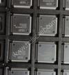
| Part Number | TS861AIDT |
|---|---|
| Manufacturer | STMicroelectronics |
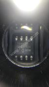
| Description | IC COMPARATOR R-R MCRPWR 8-SOIC |
| Datasheet | |
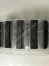
| Package | 8-SOIC (0.154", 3.90mm Width) |
| ECAD |
|
| In Stock | 55,248 piece(s) |
| Unit Price | $ 1.8994 * |
| Lead Time | Can Ship Immediately |
| Estimated Delivery Time | Apr 26 - May 1 (Choose Expedited Shipping) |
| Request for Quotation |
|
| Payment Methods | |
| Delivery Services |
Part Number # TS861AIDT (Linear - Comparators) is manufactured by STMicroelectronics and distributed by Heisener. Being one of the leading electronics distributors, we carry many kinds of electronic components from some of the world’s top class manufacturers. Their quality is guaranteed by its stringent quality control to meet all required standards.
For TS861AIDT specifications/configurations, quotation, lead time, payment terms of further enquiries please have no hesitation to contact us. To process your RFQ, please add TS861AIDT with quantity into BOM. Heisener.com does NOT require any registration to request a quote of TS861AIDT.
| Manufacturer | STMicroelectronics |
| Category | Integrated Circuits (ICs) - Linear - Comparators |
| Package | 8-SOIC (0.154", 3.90mm Width) |
| ECAD |
|
| Series | - |
| Type | General Purpose |
| Number of Elements | 1 |
| Output Type | Push-Pull |
| Voltage - Supply, Single/Dual (±) | 2.7 V ~ 10 V |
| Voltage - Input Offset (Max) | 7mV @ 5V |
| Current - Input Bias (Max) | 300pA @ 5V |
| Current - Output (Typ) | - |
| Current - Quiescent (Max) | 16µA |
| CMRR, PSRR (Typ) | 70dB CMRR |
| Propagation Delay (Max) | 2µs |
| Hysteresis | - |
| Operating Temperature | -40°C ~ 85°C |
| Package / Case | 8-SOIC (0.154", 3.90mm Width) |
| Mounting Type | Surface Mount |
| Supplier Device Package | 8-SO |
Alfre*****rtman
April 6, 2023
Madd***** Sen
April 2, 2023
Rayd*****tein
March 18, 2023
Dan*****andit
March 10, 2023


|
24980703733504F | Dialight, LED PANEL IND YLW 10V STOVEPIPE, -, - | View |
|
|
ERM 1-270 | Bivar Inc., LED MT SR VERT X 0.270" UNIV, -, - | View |
|
|
3455RC 81740208 | Honeywell Sensing and Productivity Solutions, AUTO RESET THERMOSTAT, Cylinder, - | View |

|
NPC-1210-100D-3-S | Amphenol Advanced Sensors, SENSOR PRES 100PSIA 0-100MV DIP, 8-DIP Module, - | View |

|
59065-2-T-01-C | Littelfuse Inc., SENSOR REED SW SPST-NO W LEADS, Cylinder, Threaded, - | View |

|
RNC50H5761FRBSL | Vishay Dale, RES 5.76K OHM 1/10W 1% AXIAL, Axial, - | View |

|
MNR04M0APJ180 | Rohm Semiconductor, RES ARRAY 4 RES 18 OHM 0804, 0804, Convex, Long Side Terminals, - | View |

|
PC-50100R0KE66BKT | Vishay Dale, RES CHAS MNT 100 OHM 10%, Radial, Rectangular Case, - | View |
|
|
09565515512 | HARTING, CONN D-SUB HD RCPT 78P VERT SLDR, -, - | View |

|
5-66504-6 | TE Connectivity AMP Connectors, CONN SOCKET 20-24AWG GOLD CRIMP, -, - | View |
|
|
TVPS00RF-15-97PA-LC | Amphenol Aerospace Operations, CONN RCPT HSG MALE 12POS PNL MT, -, - | View |
|
|
SI5351A-B05569-GTR | Silicon Labs, I2C PROG, ANY FREQUENCY, ANY OUT, -, - | View |

We guarantee 100% customer satisfaction.
Our experienced sales team and tech support team back our services to satisfy all our customers.

We provide 90 days warranty.
If the items you received were not in perfect quality, we would be responsible for your refund or replacement, but the items must be returned in their original condition.
| Part Number | Manufacturer | Description | Stock |
TS861AIDT D# V36:1790_06549322 |
STMicroelectronics |
Comparator Single R-R I/P 10V 8-Pin SO N T/R RoHS: Compliant
|
0 |
| Part Number | Manufacturer | Description | Stock |
TS861AIDT D# TS861AIDT |
STMicroelectronics |
Comparator Single R-R I/P 10V 8-Pin SO N T/R - Tape and Reel (Alt: TS861AIDT) |
0 |
| Part Number | Manufacturer | Description | Stock |
TS861AIDT D# TS861AIDT |
STMicroelectronics |
Comparator Single R-R I/P 10V 8-Pin SO N T/R (Alt: TS861AIDT) |
0 |
| Part Number | Manufacturer | Description | Stock |
TS861AIDT |
STMicroelectronics |
Min Qty 254 |
0 |
| Part Number | Manufacturer | Description | Stock |
TS861AIDT D# 497-8130-1-ND |
STMicroelectronics |
IC COMPARATOR R-R MCRPWR 8-SOIC |
1094 |
| Part Number | Manufacturer | Description | Stock |
TS861AIDT |
STMicroelectronics |
In stock shipping within 2days |
20260 |
| Part Number | Manufacturer | Description | Stock |
TS861AIDT |
STMicroelectronics |
IC COMPARATOR R-R MCRPWR 8-SOIC RoHS: Compliant
pbFree: Yes
|
0 |
| Part Number | Manufacturer | Description | Stock |
TS861AIDT |
STMicroelectronics |
OEM/CM QUOTES ONLY | NO BROKERS |
2737 |
| Part Number | Manufacturer | Description | Stock |
TS861AIDT |
STMicroelectronics |
OEM/CM Immediate delivery |
6528 |
| Part Number | Manufacturer | Description | Stock |
TS861AIDT D# 511-TS861AIDT |
STMicroelectronics |
Analog Comparators Single Rail-to-Rail RoHS: Compliant
|
3956 |
| Part Number | Manufacturer | Description | Stock |
TS861AIDT D# 57P4454 |
STMicroelectronics |
LGS VIPOWER RoHS: Not Compliant
Min Qty: 5000
Container: TAPE & REEL - FULL
|
0 |
| Part Number | Manufacturer | Description | Stock |
TS861AIDT D# NS-TS861AIDT |
STMicroelectronics |
OEM/CM ONLY |
7046 |
| Part Number | Manufacturer | Description | Stock |
TS861AIDT |
STMicroelectronics |
OEM/CM ONLY |
2316 |
| Part Number | Manufacturer | Description | Stock |
TS861AIDT |
STMicroelectronics |
IN stock Immediate delivery |
6543 |
Heisener's commitment to quality has shaped our processes for sourcing, testing, shipping, and every step in between. This foundation underlies each component we sell.

Do you have any question about TS861AIDT?
86-755-83210559-819


Scan to view this page