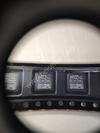
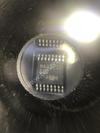
Part Number | XC6123E740ER-G |
---|---|
Manufacturer | Torex Semiconductor Ltd |
Description | IC WATCHDOG TIMER 6-USP |
Datasheet | XC6123E740ER-G Datasheet |
Package | 6-UFDFN Exposed Pad |
In Stock | 276 piece(s) |
Unit Price | $ 0.4816 * |
Lead Time | To be Confirmed |
Estimated Delivery Time | Jan 19 - Jan 24 (Choose Expedited Shipping) |
Request for Quotation |
|
Part Number # XC6123E740ER-G (PMIC - Supervisors) is manufactured by Torex Semiconductor Ltd and distributed by Heisener. Being one of the leading electronics distributors, we carry many kinds of electronic components from some of the world’s top class manufacturers. Their quality is guaranteed by its stringent quality control to meet all required standards.
For XC6123E740ER-G specifications/configurations, quotation, lead time, payment terms of further enquiries please have no hesitation to contact us. To process your RFQ, please add XC6123E740ER-G with quantity into BOM. Heisener.com does NOT require any registration to request a quote of XC6123E740ER-G.
Manufacturer | Torex Semiconductor Ltd |
Category | Integrated Circuits (ICs) - PMIC - Supervisors |
Datasheet | XC6123E740ER-GDatasheet |
Package | 6-UFDFN Exposed Pad |
Series | - |
Type | Watchdog Circuit |
Number of Voltages Monitored | 1 |
Output | Open Drain or Open Collector |
Reset | Active Low |
Reset Timeout | 800 ms Typical |
Voltage - Threshold | 4V |
Operating Temperature | -40°C ~ 85°C (TA) |
Mounting Type | Surface Mount |
Package / Case | 6-UFDFN Exposed Pad |
Supplier Device Package | 6-USPC (1.8x2) |
1/26 XC6121/XC6122 XC6123/XC6124 Series Voltage Detector with Watchdog Function and ON/OFF Control (VDF=1.6V~5.0V) 0 2.0 4.0 6.0 8.0 10.0 12.0 14.0 0 1 2 3 4 5 6 Input Voltage: VIN (V) S u p p ly C u rr e n t: I S S ( μ A ) XC6121~XC6124(VDF=2.7V) Ta=85℃ Ta=-40℃ Ta=25℃ ■GENERAL DESCRIPTION The XC6121/XC6122/XC6123/XC6124 series is a group of high-precision, low current consumption voltage detectors with watchdog functions incorporating CMOS process technology. The series consist of a reference voltage source, delay circuit, comparator, and output driver. With the built-in delay circuit, the series do not require any external components to output signals with release delay time. The output type is VDFL low when detected. The EN/ENB pin can control ON and OFF of the watchdog functions. By setting the EN/ENB pin to low or high level, the watchdog function can be OFF while the voltage detector remains operation. Since the EN/ENB pin of the XC6122 and XC6124 series is internally pulled up to the VIN pin or pulled down to the VSS pin, these series can be used with the EN/ENB pin left open when the watchdog functions is used. The detect voltages are internally fixed 1.6V ~ 5.0V in increments of 0.1V, using laser trimming technology. Six watchdog timeout periods are available in a range from 50ms to 1.6s. Five release delay times are available in a range from 3.13ms to 400ms. ■FEATURES Detect Voltage Range : 1.6V ~ 5.0V, +2% (0.1V increments) Hysteresis Width : VDFL x 5% (TYP.) Operating Voltage Range : 1.0V ~ 6.0V Detect Voltage Temperature Characteristics : +100ppm/OC (TYP.) Output Configuration : N-channel open drain Watchdog Pin : Watchdog input If watchdog input maintains ‘H’ or ‘L’ within the watchdog timeout period, a reset signal is output from the RESETB pin. EN/ENB Pin : When the EN/ENB pin voltage is set to low or high level, the watchdog function is forced off. Release Delay Time : 400ms, 200ms, 100ms, 50ms, 3.13ms (TYP.) Watchdog Timeout Period : 1.6s, 800ms, 400ms, 200ms, 100ms, 50ms (TYP.) Operating Ambient Temperature Packages Environmentally Friendly : -40℃~ +85℃ : SOT-25, USP-6C : EU RoHS Compliant, Pb Free ■APPLICATIONS ●Microprocessor watchdog monitoring and reset circuits ●Memory battery backup circuits ●System power-on reset circuits ●Power failure detection ■TYPICAL APPLICATION CIRCUIT ■TYPICAL PERFORMANCE CHARACTERISTICS ●Supply Current vs. Input Voltage ETR0209-011b
2/26 XC6121/XC6122/XC6123/XC6124 Series PIN NUMBER PIN NAME FUNCTION SOT-25 USP-6C 1 4 RESETB Reset Output 2 5 VSS Ground 3 2 EN/ENB Watchdog ON/OFF Control 4 1 WD Watchdog 5 6 VIN Power Input - 3 NC No Connection ■PIN CONFIGURATION SOT-25 (TOP VIEW) USP-6C (BOTTOM VIEW) * The dissipation pad for the USP-6C package should be solder-plated in reference mount pattern and metal masking so as to enhance mounting strength and heat release. If the pad needs to be connected to other pins, it should be connected to the VSS (No. 5) pin. ■PIN ASSIGNMENT
3/26 XC6121/XC6122/XC6123/XC6124 Series SERIES RESET OUTPUT HYSTERESIS EN/ENB PIN FUNCTION VDFL (RESETB) (*1) VDFH (RESET) EN/ENB Input Logic (*2) Pull-Up or Down Resistor XC6121 N-channel open drain - Available: VDFL x 5% (TYP.) EN With No Pull-Up Resistor XC6122 N-channel open drain - EN With Pull-Up Resistor XC6123 N-channel open drain - ENB With No Pull-Down Resistor XC6124 N-channel open drain - ENB With Pull-Down Resistor (*1) The output type of RESETB is set to L level at the time of detection. (*2) EN input logic: The watchdog function turns on when the EN pin becomes high level. ENB input logic: The watchdog function turns on when the ENB pin becomes low level. DESIGNATOR ITEM SYMBOL DESCRIPTION ① Release Delay Time(*1) A 3.13ms (TYP.) C 50ms (TYP.) D 100ms (TYP.) E 200ms (TYP.) F 400ms (TYP.) ② Watchdog Timeout Period 2 50ms (TYP.) 3 100ms (TYP.) 4 200ms (TYP.) 5 400ms (TYP.) 6 1.6s (TYP.) 7 800ms (TYP.) ③④ Detect Voltage 16 ~ 50 Detect voltage ex.) 4.5V: ③⇒4, ④⇒5 ⑤⑥-⑦(*2) Packages (Order Unit) MR SOT-25 (3,000/Reel) MR-G SOT-25 (3,000/Reel) ER USP-6C (3,000/Reel) ER-G USP-6C (3,000/Reel) ■PRODUCT CLASSIFICATION ●Selection Guide ●Ordering Information XC6121①②③④⑤⑥-⑦(*2): N-channel Open Drain Output (RESETB), EN Pin: No Pull-Up Resistor XC6122①②③④⑤⑥-⑦(*2): N-channel Open Drain Output (RESETB), EN Pin: Pull-Up Resistor XC6123①②③④⑤⑥-⑦(*2): N-channel Open Drain Output (RESETB), ENB Pin: No Pull-Down Resistor XC6124①②③④⑤⑥-⑦(*2): N-channel Open Drain Output (RESETB), ENB Pin: Pull-Down Resistor (*1) Please set the release delay time shorter than or equal to the watchdog timeout period. ex.) XC6121D327MR or XC6121D627MR (*2) The “-G” suffix denotes Halogen and Antimony free as well as being fully EU RoHS compliant.
4/26 XC6121/XC6122/XC6123/XC6124 Series ■BLOCK DIAGRAMS ●XC6121 Series ●XC6122 Series N-ch Open Drain Output N-ch Open Drain Output
5/26 XC6121/XC6122/XC6123/XC6124 Series ■BLOCK DIAGRAMS (Continued) ●XC6123 Series ●XC6124 Series N-ch Open Drain Output N-ch Open Drain Output
6/26 XC6121/XC6122/XC6123/XC6124 Series PARAMETER SYMBOL RATINGS UNITS Input Voltage VIN VSS -0.3 ~ 7.0 V VEN/VENB VSS-0.3~VIN+0.3≦7.0 V VWD VSS -0.3 ~ 7.0 V Output Current IRBOUT 20 mA Output Voltage VRESETB VSS -0.3 ~ 7.0 V Power Dissipation SOT-25 Pd 250 mW USP-6C 120 Operating Ambient Temperature Topr -40 ~ +85 OC Storage Temperature Tstg -55 ~ +125 OC ■ABSOLUTE MAXIMUM RATINGS Ta=25OC
7/26 XC6121/XC6122/XC6123/XC6124 Series PARAMETER SYMBOL CONDITIONS MIN. TYP. MAX. UNITS CIRCUIT Detect Voltage VDFL VEN=VSS VDFL(T) × 0.98 VDFL(T) VDFL(T) × 1.02 V ① Hysteresis Width VHYS VEN=VSS VDFL× 0.02 VDFL × 0.05 VDFL × 0.08 V ① Supply Current (*1) ISS WD=OPEN VIN=VDFL(T)×0.9V - 5 11 μA ② VIN=VDFL(T)×1.1V - 10 16 VIN=6.0V - 12 18 Operating Voltage VIN 1.0 - 6.0 V ① Output Current IRBOUT N-ch. VDS=0.5V VIN=1.0V 0.15 0.5 - mA ③ VIN=2.0V (VDFL(T)> 2.0V) 2.0 2.5 - VIN=3.0V (VDFL(T) >3.0V) 3.0 3.5 - VIN=4.0V (VDFL(T) >4.0V) 3.5 4.0 - Temperature Characteristics △VDFL / △Topr・VDFL -40 OC < Topr < 85 OC - +100 - ppm/ OC ① Release Delay Time (VDFL<1.8V) tDR Time until VIN is increased from 1.0V to 2.0V and attains to the release time level, and the Reset output pin releases. 2.00 3.13 5.00 ms ④ 37 50 63 75 100 125 150 200 250 300 400 500 Release Delay Time (VDFL>1.9V) tDR Time until VIN is increased from 1.0V to (VDFL x 1.1V) and attains to the release time level, and the Reset output pin releases. 2.00 3.13 5.00 ms ④ 37 50 63 75 100 125 150 200 250 300 400 500 Detect Delay Time tDF Time until VIN is decreased from 6.0V to 1.0V and attains to the detect voltage level, and the Reset output pin detects while the WD pin left open. - 5.5 33 μs ④ VDFL Leakage Current ILEAK VIN=6.0V, VRESETB=6.0V - 0.01 0.1 μA ③ Watchdog Timeout Period (VDFL<1.8V) tWD Time until VIN increases form 1.0V to 2.0V and the Reset output pin is released to go into the detection state. (WD=OPEN) 37 50 63 ms ⑤ 75 100 125 150 200 250 300 400 500 600 800 1000 1200 1600 2000 Watchdog Timeout Period (VDFL>1.9V) tWD Time until VIN increases from 1.0V to (VDFLx1.1V) and the Reset output pin is released to go into the detection state. (WD=OPEN) 37 50 63 ms ⑤ 75 100 125 150 200 250 300 400 500 600 800 1000 1200 1600 2000 ■ELECTRICAL CHARACTERISTICS Ta=25 OC
8/26 XC6121/XC6122/XC6123/XC6124 Series PARAMETER SYMBOL CONDITIONS MIN. TYP. MAX. UNITS CIRCUIT Watchdog Minimum Pulse Width tWDIN VIN=6.0V, Apply pulse from 6.0V to 0V to the WD pin. 300 - - ns ⑥ Watchdog High Level Voltage VWDH VIN=VDFL x 1.1V ~ 6.0V VIN x 0.7 - 6 V ⑥ Watchdog Low Level Voltage VWDL VIN=VDFL x 1.1V ~ 6.0V 0 - VIN x 0.3 V ⑥ Watchdog Pull-down Resistance RWD VWD=6V, RWD=VWD/IWD 300 600 900 kΩ ⑦ EN/ENB High Level Voltage VENH/VENBH VIN=VDFL x 1.1V ~ 6.0V 1.3 - VIN V ⑧ EN/ENB Low Level Voltage VENL/VENBL VIN=VDFL x 1.1V ~ 6.0V 0 - 0.35 V ⑧ EN Pull-up Resistance (*2) REN VIN=6.0V, VEN=0V, REN=VIN / IEN 1.0 1.6 2.4 MΩ ⑨ ENB Pull-down Resistance (*3) RENB VIN=6.0V, VENB=6V, RENB=VENB / IENB NOTE: * In case where no EN/ENB pin’s condition written in the test condition field, VEN=VIN and VENB=VSS. ** VDFL(T)=Setting detect voltage value (*1) The condition when the watchdog pin is ON. The EN/ENB pin is CMOS input. For the XC6122 (pull-up resistor) and XC6124 (pull-down resistor), supply current increases in the following values when the watchdog function is OFF. XC6122 Series:(VIN-VEHL)/1.6MΩ(TYP.) XC6124 Series:VEHBH/1.6MΩ(TYP.) (*2) For the XC6122 series only. (*3) For the XC6124 series only. ■ELECTRICAL CHARACTERISTICS (Continued) Ta=25 OC
9/26
XC6121/XC6122/XC6123/XC6124
Series
■OPERATIONAL EXPLANATION
The XC6121/6122/6123/6124 series compare, using the error amplifier, the voltage of the internal voltage reference source
with the voltage divided by R1, R2 and R3 connected to the VIN pin. The resulting output signal from the error amplifier
activates the watchdog logic, delay circuit and the output driver. When the VIN pin voltage gradually falls and finally reaches
the detect voltage, the RESETB pin output goes from high to low in the case of the VDFL type ICs.
Lex*****ogi
December 27, 2021
Eric*****okes
December 23, 2020
We guarantee 100% customer satisfaction.
Our experienced sales team and tech support team back our services to satisfy all our customers.
We provide 90 days warranty.
If the items you received were not in perfect quality, we would be responsible for your refund or replacement, but the items must be returned in their original condition.
Payment Methods | |
Delivery Services |
Heisener's commitment to quality has shaped our processes for sourcing, testing, shipping, and every step in between. This foundation underlies each component we sell.