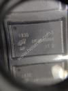
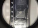
| Part Number | ZXMP3A16GTA |
|---|---|
| Manufacturer | Diodes Incorporated |
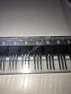
| Description | MOSFET P-CH 30V 4.6A SOT223 |
| Datasheet | |
| Package | TO-261-4, TO-261AA |
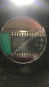
| ECAD |
|
| In Stock | 1,164,408 piece(s) |
| Unit Price | Request a Quote |
| Lead Time | Can Ship Immediately |
| Estimated Delivery Time | Apr 27 - May 2 (Choose Expedited Shipping) |
| Request for Quotation |
|
| Payment Methods | |
| Delivery Services |
Part Number # ZXMP3A16GTA (Transistors - FETs, MOSFETs - Single) is manufactured by Diodes Incorporated and distributed by Heisener. Being one of the leading electronics distributors, we carry many kinds of electronic components from some of the world’s top class manufacturers. Their quality is guaranteed by its stringent quality control to meet all required standards.
For ZXMP3A16GTA specifications/configurations, quotation, lead time, payment terms of further enquiries please have no hesitation to contact us. To process your RFQ, please add ZXMP3A16GTA with quantity into BOM. Heisener.com does NOT require any registration to request a quote of ZXMP3A16GTA.
| Manufacturer | Diodes Incorporated |
| Category | Discrete Semiconductor Products - Transistors - FETs, MOSFETs - Single |
| Package | TO-261-4, TO-261AA |
| ECAD |
|
| Series | - |
| FET Type | P-Channel |
| Technology | MOSFET (Metal Oxide) |
| Drain to Source Voltage (Vdss) | 30V |
| Current - Continuous Drain (Id) @ 25°C | 5.4A (Ta) |
| Drive Voltage (Max Rds On, Min Rds On) | 4.5V, 10V |
| Vgs(th) (Max) @ Id | 1V @ 250µA |
| Gate Charge (Qg) (Max) @ Vgs | 29.6nC @ 10V |
| Input Capacitance (Ciss) (Max) @ Vds | 1022pF @ 15V |
| Vgs (Max) | ±20V |
| FET Feature | - |
| Power Dissipation (Max) | 2W (Ta) |
| Rds On (Max) @ Id, Vgs | 45 mOhm @ 4.2A, 10V |
| Operating Temperature | -55°C ~ 150°C (TJ) |
| Mounting Type | Surface Mount |
| Supplier Device Package | SOT-223 |
| Package / Case | TO-261-4, TO-261AA |
Bro*****Manne
April 9, 2023
Adel*****mall
April 9, 2023
Migu*****errano
April 6, 2023
Rosa*****Sandal
March 26, 2023
Vincen*****amanian
March 16, 2023


|
SIT8208AC-33-25E-16.000000Y | SiTIME, -20 TO 70C, 5032, 50PPM, 2.5V, 1, -, - | View |

|
SIT1602BC-73-33N-37.500000E | SiTIME, -20 TO 70C, 2016, 50PPM, 3.3V, 3, -, - | View |
|
|
2220J1000681JFR | Knowles Syfer, CAP CER 680PF 100V C0G/NP0 2220, 2220 (5750 Metric), - | View |
|
|
1825J1000273MXT | Knowles Syfer, CAP CER 0.027UF 100V X7R 1825, 1825 (4564 Metric), - | View |
|
|
0603J0250472JDT | Knowles Syfer, CAP CER 4700PF 25V X7R 0603, 0603 (1608 Metric), - | View |

|
12101C683KAT2A | AVX Corporation, CAP CER 0.068UF 100V X7R 1210, 1210 (3225 Metric), - | View |
|
|
VS-VSKE166/04PBF | Vishay Semiconductor Diodes Division, DIODE MODULE 400V INT-A-PAK, INT-A-PAK (3), - | View |
|
|
MK3P5-S-DC48 | Omron Automation and Safety, RELAY GEN PURPOSE 3PDT 10A 48V, -, - | View |

|
8532R-31L | API Delevan Inc., FIXED IND 330UH 740MA 650 MOHM, Nonstandard, - | View |
|
|
MS3456L12S-3SW | Amphenol Aerospace Operations, CONN PLUG 2POS STRAIGHT W/SCKT, -, - | View |
|
|
VE-25H-CY-F2 | Vicor Corporation, CONVERTER MOD DC/DC 52V 50W, Full Brick, - | View |
 
|
CP82C84A | Renesas Electronics America, IC CLK GEN 5V 25MHZ 18-DIP, 18-DIP (0.300", 7.62mm), - | View |

We guarantee 100% customer satisfaction.
Our experienced sales team and tech support team back our services to satisfy all our customers.

We provide 90 days warranty.
If the items you received were not in perfect quality, we would be responsible for your refund or replacement, but the items must be returned in their original condition.
| Part Number | Manufacturer | Description | Stock |
ZXMP3A16GTA D# 70438856 |
Diodes Incorporated |
MOSFET P-Channel 30V 7.5A SOT223 RoHS: Not Compliant
|
0 |
| Part Number | Manufacturer | Description | Stock |
ZXMP3A16GTA D# E02:0323_01118391 |
Zetex / Diodes Inc |
Trans MOSFET P-CH 30V 5.4A 4-Pin(3+Tab) SOT-223 T/R |
0 |
| Part Number | Manufacturer | Description | Stock |
ZXMP3A16GTA D# ZXMP3A16GTA |
Diodes Incorporated |
Trans MOSFET P-CH 30V 7.5A 4-Pin(3+Tab) SOT-223 T/R - Tape and Reel (Alt: ZXMP3A16GTA) RoHS: Compliant
|
0 |
| Part Number | Manufacturer | Description | Stock |
ZXMP3A16GTA D# ZXMP3A16GTA |
Diodes Incorporated |
Trans MOSFET P-CH 30V 7.5A 4-Pin(3+Tab) SOT-223 T/R (Alt: ZXMP3A16GTA) RoHS: Compliant
|
0 |
| Part Number | Manufacturer | Description | Stock |
ZXMP3A16GTA D# ZXMP3A16GTA |
Diodes Incorporated |
Trans MOSFET P-CH 30V 7.5A 4-Pin(3+Tab) SOT-223 T/R (Alt: ZXMP3A16GTA) RoHS: Compliant
|
0 |
| Part Number | Manufacturer | Description | Stock |
ZXMP3A16GTA |
Zetex / Diodes Inc | 1031 |
| Part Number | Manufacturer | Description | Stock |
ZXMP3A16GTA |
Diodes Incorporated |
MOSFET Transistor, P-Channel, SO |
747 |
| Part Number | Manufacturer | Description | Stock |
ZXMP3A16GTA |
Diodes Incorporated |
P-Channel 30V 5.4A 1V @ 250uA 45mohms @ 4.2A,10V 2W SOT-223 MOSFET RoHS |
1151 |
| Part Number | Manufacturer | Description | Stock |
ZXMP3A16GTA |
Diodes Incorporated |
RoHS: Compliant
|
0 |
| Part Number | Manufacturer | Description | Stock |
ZXMP3A16GTA D# ZXMP3A16GCT-ND |
Diodes Incorporated |
MOSFET P-CH 30V 5.4A SOT223 |
29787 |
| Part Number | Manufacturer | Description | Stock |
ZXMP3A16GTA |
ZETEX |
In stock shipping within 2days |
33525 |
| Part Number | Manufacturer | Description | Stock |
ZXMP3A16GTA D# 2061511RL |
Diodes Incorporated |
MOSFET, P CH, 30V, 5.4A, SOT223 RoHS: Compliant
Min Qty: 1
Container: Reel
|
0 |
| Part Number | Manufacturer | Description | Stock |
ZXMP3A16GTA |
Diodes Incorporated |
P-Channel 30 V 0.045 Ohm Enhancement Mode MOSFET - SOT-223 RoHS: Compliant
pbFree: Yes
|
0 |
| Part Number | Manufacturer | Description | Stock |
ZXMP3A16GTA |
DIODES INCORPORATED |
OEM/CM QUOTES ONLY | NO BROKERS |
48790 |
| Part Number | Manufacturer | Description | Stock |
ZXMP3A16GTA |
Zetex / Diodes Inc |
In stock |
74 |
| Part Number | Manufacturer | Description | Stock |
ZXMP3A16GTA D# C260929 |
Diodes Incorporated | 1141 |
| Part Number | Manufacturer | Description | Stock |
ZXMP3A16GTA |
Diodes Incorporated |
OEM/CM Immediate delivery |
180000 |
| Part Number | Manufacturer | Description | Stock |
ZXMP3A16GTA D# 522-ZXMP3A16GTA |
Diodes Incorporated |
MOSFET 30V P Chnl UMOS RoHS: Compliant
|
6096 |
| Part Number | Manufacturer | Description | Stock |
ZXMP3A16GTA D# XSFP00000079007 |
Diodes Incorporated |
P-Channel 30 V 0.045 Ohm Enhancement Mode MOSFET - SOT-223 |
17000 |
| Part Number | Manufacturer | Description | Stock |
ZXMP3A16GTA D# 65T9555 |
Diodes Incorporated |
MOSFET, P CHANNEL, 30V, 5.4A, SOT223, Transistor Polarity:P Channel, Drain Source Voltage Vds:30V, Continuous Drain Current Id:5.4A, On Resistance Rds(on):0.045ohm, Transistor Mounting:Surface Mount, Rds(on) Test Voltage Vgs:10V RoHS Compliant: Yes RoHS: Compliant
Min Qty: 1
Container: Cut Tape
|
744 |
| Part Number | Manufacturer | Description | Stock |
ZXMP3A16GTA D# NS-ZXMP3A16GTA |
Diodes Incorporated |
OEM/CM ONLY |
16013 |
ZXMP3A16GTA-CT D# NS-ZXMP3A16GTA-CT |
Zetex Inc |
OEM/CM ONLY |
1815 |
| Part Number | Manufacturer | Description | Stock |
ZXMP3A16GTA |
Zetex / Diodes Inc |
MOSFET Transistor, P-Channel, SO |
33 |
| Part Number | Manufacturer | Description | Stock |
ZXMP3A16GTA D# 7082545P |
Zetex / Diodes Inc |
P-Channel MOSFET, 7.5 A, 30 V, 3 + Tab-Pin SOT-223 Diodes Inc ZXMP3A16GTA, RL Min Qty: 5
Container: Reel
|
1350 |
| Part Number | Manufacturer | Description | Stock |
ZXMP3A16GTA D# TMOSS6745 |
Diodes Incorporated |
P-CH 30V 7,5A 45mOhm SOT223 RoHS: Compliant
|
0 |
| Part Number | Manufacturer | Description | Stock |
ZXMP3A16GTA |
Zetex / Diodes Inc |
OEM/CM ONLY |
15053 |
| Part Number | Manufacturer | Description | Stock |
ZXMP3A16GTA |
Diodes Incorporated |
IN stock Immediate delivery |
179985 |
| Part Number | Manufacturer | Description | Stock |
ZXMP3A16GTA |
Diodes Incorporated |
shipping today |
54 |
| Part Number | Manufacturer | Description | Stock |
ZXMP3A16GTA D# 50130759 |
Zetex / Diodes Inc |
Trans MOSFET P-CH 30V 5.4A 4-Pin(3+Tab) SOT-223 T/R |
0 |
| Part Number | Manufacturer | Description | Stock |
ZXMP3A16GTA |
mfr |
RFQ |
7411 |
| Part Number | Manufacturer | Description | Stock |
ZXMP3A16GTA D# 2061511 |
Diodes Incorporated |
MOSFET, P CH, 30V, 5.4A, SOT223 RoHS: Compliant
Min Qty: 1
Container: Cut Tape
|
1037 |
Heisener's commitment to quality has shaped our processes for sourcing, testing, shipping, and every step in between. This foundation underlies each component we sell.

Do you have any question about ZXMP3A16GTA?
+86-755-83210559-836


Scan to view this page