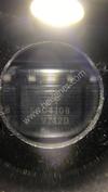
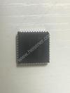
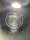
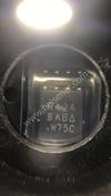
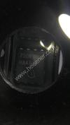
| Part Number | ZXMP3A17DN8TA |
|---|---|
| Manufacturer | Diodes Incorporated |
| Description | MOSFET 2P-CH 30V 3.4A 8-SOIC |
| Datasheet | |
| Package | 8-SOIC (0.154", 3.90mm Width) |
| ECAD |
|
| In Stock | 501,216 piece(s) |
| Unit Price | Request a Quote |
| Lead Time | Can Ship Immediately |
| Estimated Delivery Time | Apr 26 - May 1 (Choose Expedited Shipping) |
| Request for Quotation |
|
| Payment Methods | |
| Delivery Services |
Part Number # ZXMP3A17DN8TA (Transistors - FETs, MOSFETs - Arrays) is manufactured by Diodes Incorporated and distributed by Heisener. Being one of the leading electronics distributors, we carry many kinds of electronic components from some of the world’s top class manufacturers. Their quality is guaranteed by its stringent quality control to meet all required standards.
For ZXMP3A17DN8TA specifications/configurations, quotation, lead time, payment terms of further enquiries please have no hesitation to contact us. To process your RFQ, please add ZXMP3A17DN8TA with quantity into BOM. Heisener.com does NOT require any registration to request a quote of ZXMP3A17DN8TA.
| Manufacturer | Diodes Incorporated |
| Category | Discrete Semiconductor Products - Transistors - FETs, MOSFETs - Arrays |
| Package | 8-SOIC (0.154", 3.90mm Width) |
| ECAD |
|
| Series | - |
| FET Type | 2 P-Channel (Dual) |
| FET Feature | Logic Level Gate |
| Drain to Source Voltage (Vdss) | 30V |
| Current - Continuous Drain (Id) @ 25°C | 3.4A |
| Rds On (Max) @ Id, Vgs | 70 mOhm @ 3.2A, 10V |
| Vgs(th) (Max) @ Id | 1V @ 250µA (Min) |
| Gate Charge (Qg) (Max) @ Vgs | 15.8nC @ 10V |
| Input Capacitance (Ciss) (Max) @ Vds | 630pF @ 15V |
| Power - Max | 1.8W |
| Operating Temperature | -55°C ~ 150°C (TJ) |
| Mounting Type | Surface Mount |
| Package / Case | 8-SOIC (0.154", 3.90mm Width) |
| Supplier Device Package | 8-SOP |
Lain*****tevens
March 25, 2023
Bryce*****amillo
February 27, 2023


|
1825J4K00330GCR | Knowles Syfer, CAP CER 33PF 4KV C0G/NP0 1825, 1825 (4564 Metric), - | View |
|
|
1210J0250271GCT | Knowles Syfer, CAP CER 270PF 25V C0G/NP0 1210, 1210 (3225 Metric), - | View |

|
LMK042BJ151KC-W | Taiyo Yuden, CAP CER 150PF 10V X5R 01005, 01005 (0402 Metric), - | View |

|
HSMS-286B-TR2G | Broadcom Limited, DIODE SCHOTTKY DETECT HF SOT-323, SC-70, SOT-323, - | View |

|
MC100EL39DWR2G | ON Semiconductor, IC CLOCK GEN 2 4/6 ECL 20-SOIC, 20-SOIC (0.295", 7.50mm Width), - | View |

|
RG1608N-1131-B-T5 | Susumu, RES SMD 1.13KOHM 0.1% 1/10W 0603, 0603 (1608 Metric), - | View |

|
2139 | Adafruit Industries LLC, 2.54MM/0.1 PITCH TERMINAL BLOCK, -, - | View |
|
|
V51351510000G | Amphenol Anytek, TERM BLOCK RCPT 13POS 5.08MM, -, - | View |
|
|
ERM8-025-05.0-S-DV-DSP-K-TR | Samtec Inc., .8MM EDGE RATE TERMINAL ASSEMBLY, -, - | View |
|
|
D38999/24MB2JA | TE Connectivity Deutsch Connectors, CONN RCPT 2POS JAM NUT W/SKT, -, - | View |
|
|
RCM12DRST-S664 | Sullins Connector Solutions, CONN EDGE DUAL FMALE 24POS 0.156, -, - | View |

|
ISL54006IRTZ | Renesas Electronics America, IC AMP AUDIO PWR 1.23W AB 20TQFN, 20-WFQFN Exposed Pad, - | View |

We guarantee 100% customer satisfaction.
Our experienced sales team and tech support team back our services to satisfy all our customers.

We provide 90 days warranty.
If the items you received were not in perfect quality, we would be responsible for your refund or replacement, but the items must be returned in their original condition.
| Part Number | Manufacturer | Description | Stock |
ZXMP3A17DN8TA D# V36:1790_06708133 |
Zetex / Diodes Inc |
Trans MOSFET P-CH 30V 4.4A 8-Pin SOIC T/R RoHS: Compliant
|
0 |
| Part Number | Manufacturer | Description | Stock |
ZXMP3A17DN8TA D# ZXMP3A17DN8TA |
Diodes Incorporated |
Transistor MOSFET Array Dual P-CH 30V 4.4A 8-Pin SOIC T/R - Tape and Reel (Alt: ZXMP3A17DN8TA) RoHS: Compliant
|
0 |
| Part Number | Manufacturer | Description | Stock |
ZXMP3A17DN8TA D# ZXMP3A17DN8TA |
Diodes Incorporated |
Transistor MOSFET Array Dual P-CH 30V 4.4A 8-Pin SOIC T/R (Alt: ZXMP3A17DN8TA) |
0 |
| Part Number | Manufacturer | Description | Stock |
ZXMP3A17DN8TA |
Diodes Incorporated |
MOSFET 2P-CH 30V 3.4A 8-SOIC |
2000 |
| Part Number | Manufacturer | Description | Stock |
ZXMP3A17DN8TA D# ZXMP3A17DN8CT-ND |
Diodes Incorporated |
MOSFET 2P-CH 30V 3.4A 8-SOIC |
1 |
| Part Number | Manufacturer | Description | Stock |
ZXMP3A17DN8TA |
VBsemi Electronics Co Ltd |
In stock shipping within 2days |
17845 |
| Part Number | Manufacturer | Description | Stock |
ZXMP3A17DN8TA |
Diodes Incorporated |
Dual P-Channel 30 V 0.07 Ohm Enhancement Mode MOSFET - SOIC-8 RoHS: Compliant
pbFree: Yes
|
0 |
| Part Number | Manufacturer | Description | Stock |
ZXMP3A17DN8TA |
Zetex / Diodes Inc |
OEM/CM QUOTES ONLY | NO BROKERS |
1785 |
| Part Number | Manufacturer | Description | Stock |
ZXMP3A17DN8TA |
Diodes Incorporated |
OEM/CM Immediate delivery |
180000 |
| Part Number | Manufacturer | Description | Stock |
ZXMP3A17DN8TA D# 522-ZXMP3A17DN8TA |
Diodes Incorporated |
MOSFET Dl 30V P-Chnl UMOS RoHS: Compliant
|
345 |
| Part Number | Manufacturer | Description | Stock |
ZXMP3A17DN8TA D# NS-ZXMP3A17DN8TA |
Diodes Incorporated |
OEM/CM ONLY |
2513 |
| Part Number | Manufacturer | Description | Stock |
ZXMP3A17DN8TA |
Zetex / Diodes Inc |
OEM/CM ONLY |
4015 |
| Part Number | Manufacturer | Description | Stock |
ZXMP3A17DN8TA |
Diodes Incorporated |
IN stock Immediate delivery |
179985 |
| Part Number | Manufacturer | Description | Stock |
ZXMP3A17DN8TA |
Zetex / Diodes Inc |
shipping today |
490 |
| Part Number | Manufacturer | Description | Stock |
ZXMP3A17DN8TA |
mfr |
RFQ |
3453 |
Heisener's commitment to quality has shaped our processes for sourcing, testing, shipping, and every step in between. This foundation underlies each component we sell.

Do you have any question about ZXMP3A17DN8TA?
+86-755-83210135-818


Scan to view this page