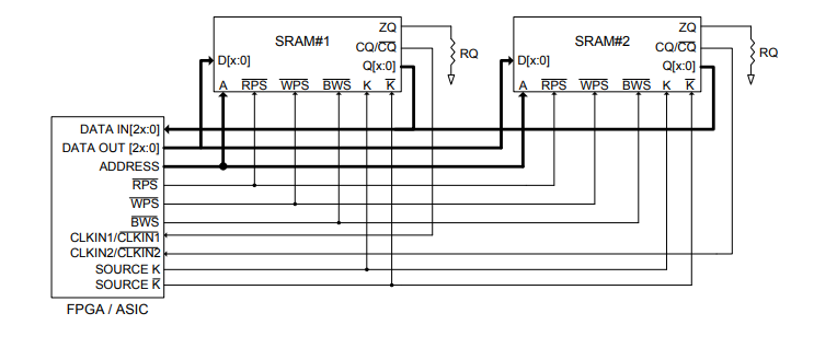
The CY7C1263KV18 and CY7C1265KV18 are 1.8V synchronous pipelined sram with QDR II+ architecture. Similar to the QDR II architecture, the QDR II+ architecture consists of two separate ports: a read port and a write port for accessing memory arrays. A read port has a special data output to support read operations, and a write port has a special data input to support write operations. The QDR II+ architecture has separate data input and output, completely eliminating the need for a data bus to "turn around" common I/O devices. Each port is accessed through a common address bus.
CY7C1263KV18 logical block diagram

CY7C1265KV18 logical block diagram
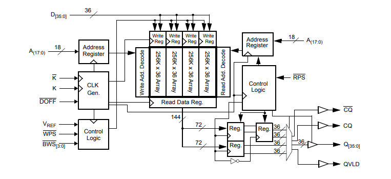
The address locks that read and write addresses exist on the alternating rising edge of the input (K) clock. QDR II+ read/write port access is completely independent. To maximize data throughput, both read and write ports are equipped with DDR interfaces. Each address location is associated with four 18-bit words (CY7C1263KV18) or 36-bit words (CY7C1265KV18), which in turn enter or output the device.
Since data flows in and out of the device on each rising edge of the two input clocks (K and K), memory bandwidth is maximized while simplifying system design by eliminating bus "turnover." Depth expansion is achieved through port selection, so that each port operates independently. All synchronous inputs pass through an input register controlled by a K or K input clock. All data output passes through an output register controlled by a K or K input clock.
Application example diagram