B85RS2MTA is a FRAM (Ferroelectric Random Access Memory) chip in a configuration of 262,144 words 8 bits, using the ferroelectric process and silicon gate CMOS process technologies for forming the nonvolatile memory cells.
& ;
MB85RS2MTA adopts the Serial Peripheral Interface (SPI).
& ;
The MB85RS2MTA is able to retain data without using a back-up battery, as is needed for SRAM.
& ;
The memory cells used in the MB85RS2MTA can be used for 1013 read/write operations, which is a significant improvement over the number of read and write operations supported by Flash memory and E2 PROM. MB85RS2MTA does not take long time to write data like Flash memories or E2 PROM, and MB85RS2MTA takes no wait time.
& ;
■
FEATURES
• & ;Bit configuration : 262,144 words 8 bits
• & ;Serial Peripheral Interface: SPI (Serial Peripheral Interface)
Correspondent to SPI mode 0 (0, 0) and mode 3 (1, 1)
• & ;Operating frequency: 40MHz (Max)
• & ;High endurance: 1013& ;times / byte
• & ;Data retention: 10 years (+85℃)
• & ;Operating power supply voltage : 1.8 V to 3.6 V
• & ;Low power consumption : Operating power supply current 2.0 mA (Max@40 MHz)
Standby current 50μA (Max)
Sleep current 10μA (Max)
• & ;Operation ambient temperature range : -40℃ to +85℃
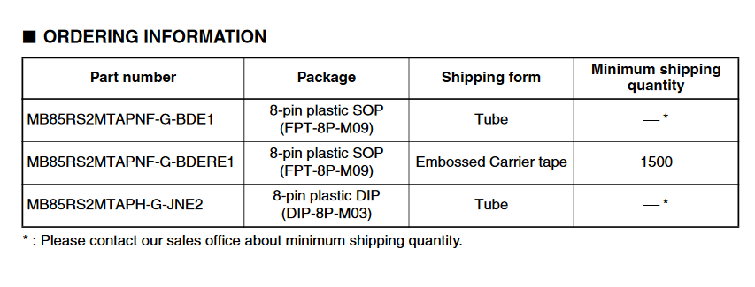
• & ;Package : 8-pin plastic SOP (FPT-8P-M09)
8-pin plastic DIP (DIP-8P-M03)
RoHS compliant