Anson Semiconductor has released a pair of 1200V all-sic MOSFET 2-Pack modules, further enhancing their product range to suit the challenging electric vehicle market.
Based on planar technology, the new module is well suited to drive voltages in the 18-20V range and can be easily driven with negative gate voltages. The larger bare sheet reduces thermal resistance compared to a grooved MOSFEts and thus reduces the bare sheet temperature at the same operating temperature.
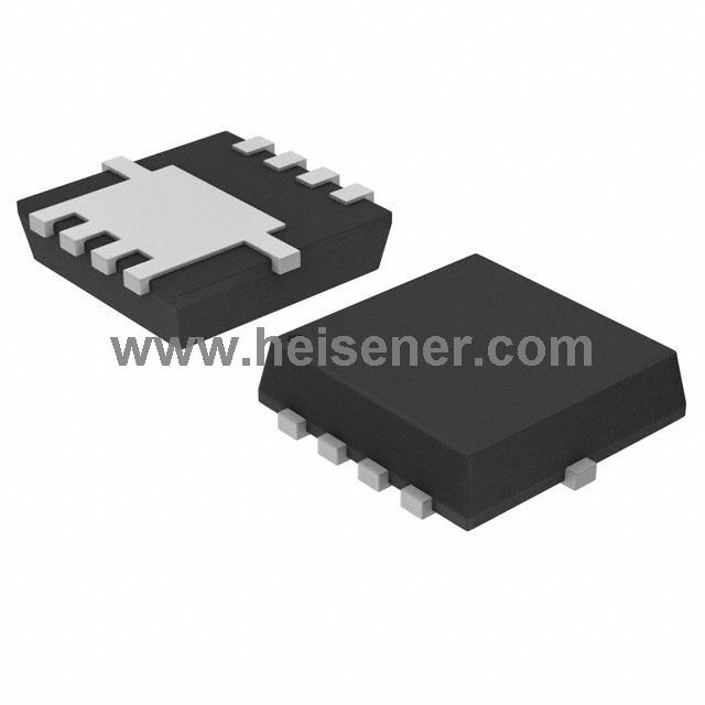
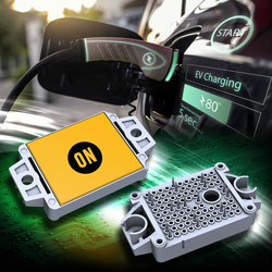
The NXH010P120MNF is configured as a 2-pack half-bridge, which is a 10mOhm device included in the F1 package, while the NXH006P120MNF2 is a 6mOhm device included in the F2 package. The package features press-off pins, making it ideal for industrial applications, and built-in NTC thermistors for easy temperature monitoring.
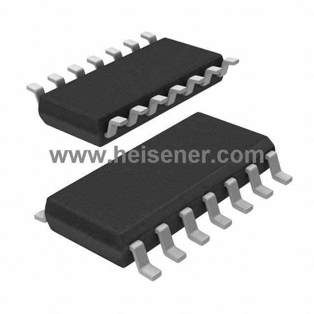
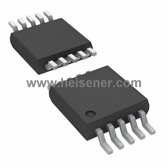
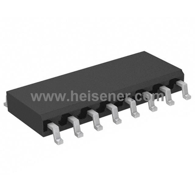
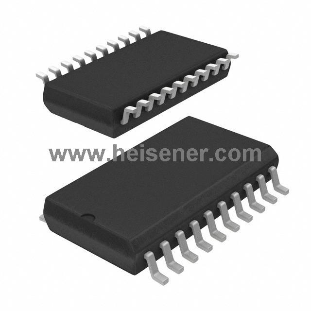
The new SiC MOSFET modules are already operating with drive solutions such as the NCD5700x devices as part of the company's EV charging ecosystem. The recently introduced NCD57252 dual-channel isolated IGBT/MOSFET gate driver provides 5kV of galvanic isolation and can be configured for dual low-side, dual high-side or half-bridge operation.
The NCD57252 comes in a small SOIC-16 wide-body package and can receive logic level inputs (3.3V, 5V and 15V). With a typical propagation delay of 60ns, high-current devices (drawing current 4A at miller platform voltage/filling current 6A) are ideal for high-speed operation.
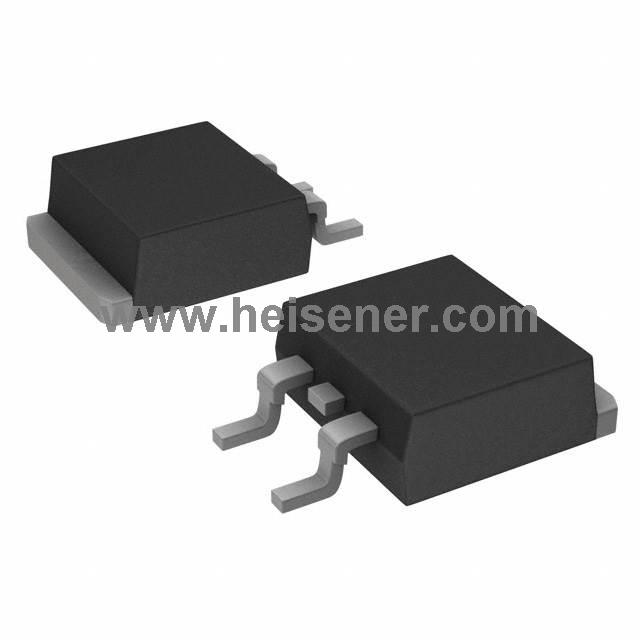
Devices in the 650V SiC MOSFET series include NVBG015N065SC1, NTBG015N065SC1, NVH4L015N065SC1 and NTH4L015N065SC, Provides the lowest RDS(on) on the market for D2PAK7L/TO247 packaged mosfets. Is recently released, using a novel active cell design combined with advanced thin wafer technology to provide first-class FoM for (RDS(ON)*area).
The 1200V and 900V N-channel SiC MOSFEts provide a small chip size that reduces switching losses when operating at the high frequencies required for ev chargers, and also reduces device capacitance and gate charge (Qg - as low as 220nC)