Nexperia, the high-throughput production specialist in basic semiconductor devices, today announced the PMCB60XN and PMCB60XNE 30V N-Channel Small Signal Trench MOSFETs in an ultra-compact wafer-level DSN1006 package with market-leading RDS(on) characteristics in space-constrained Long-lasting power in situations where battery life and battery life are critical.
The new MOSFETs are ideal for highly miniaturized electronics such as smartphones, smart watches, hearing aids, and headphones, catering to the trend toward smarter, more feature-rich, and increasing system power consumption.RDS(on) improves performance by 25% compared to competing devices, minimizing power consumption and improving load switching and battery management efficiency. Its excellent performance is also reflected in the reduction of self-heating, thereby enhancing the user comfort of wearable devices.
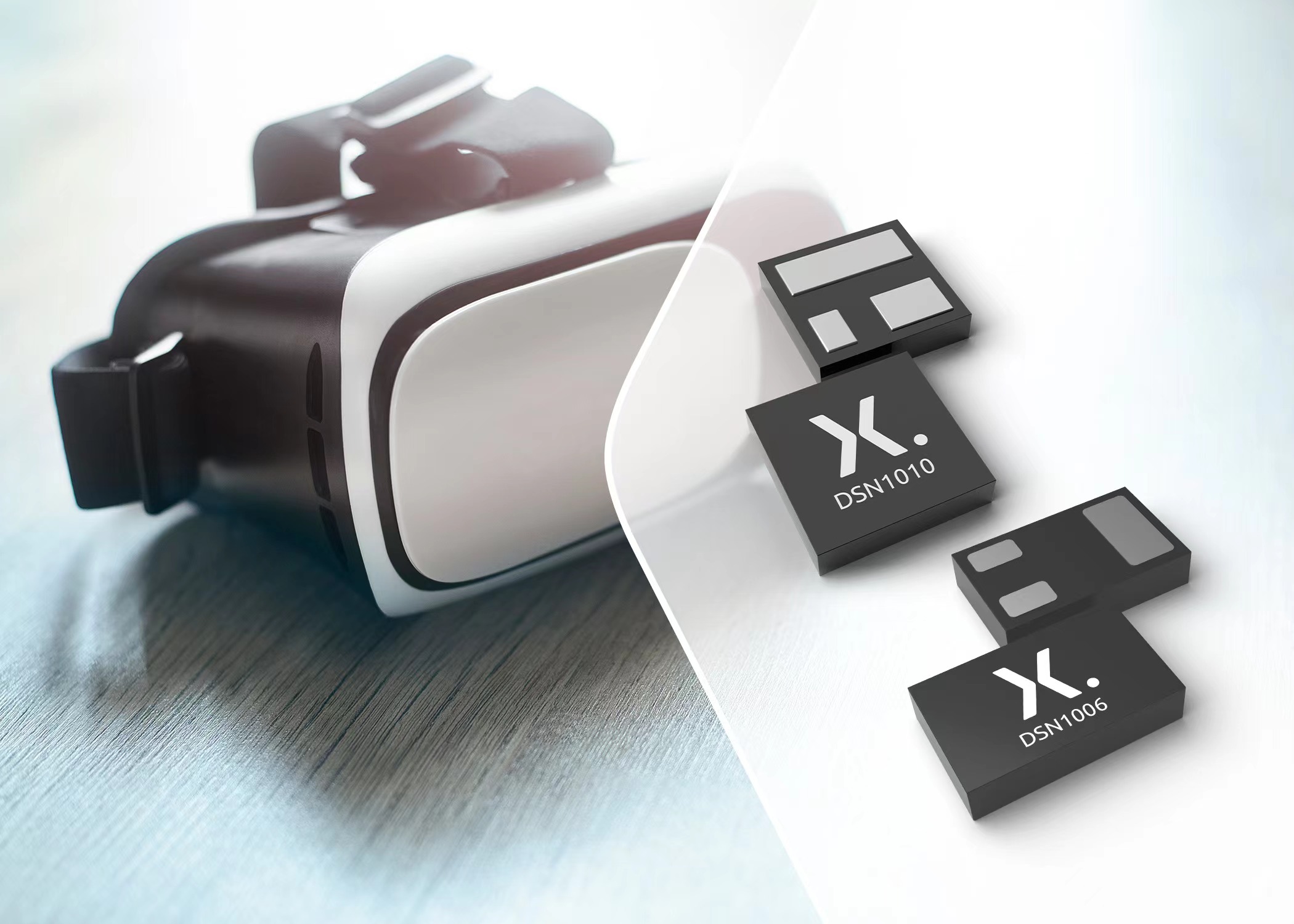
Specifically, at VGS = 4.5V, the maximum RDS(on) of PMCB60XN and PMCB60XNE are 50mΩ and 55mΩ, respectively. Therefore, among similar 30V MOSFETs on the market, the PMCB60XN and PMCB60XNE have the lowest on-resistance per die area. In addition, the PMCB60XNE offers 2kV ESD protection (Human Body Model – HBM) rated in the DSN1006 small form factor of 1.0mm × 0.6mm × 0.2mm. Both MOSFETs are rated for drain currents up to 4A.
In addition to these two MOSFETs in the DSN1006 package, Nexperia also introduced a 12V N-channel Trench MOSFET PMCA14UN in the DSN1010 package. The PMCA14UN has a maximum RDS(on) of 16mΩ at VGS = 4.5 V and market-leading efficiency in a 0.96mm × 0.96mm × 0.24mm (SOT8007) size.