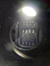
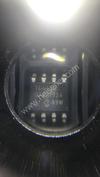
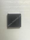
Page 1
Page 2
REV. B
Information furnished by Analog Devices is believed to be accurate and
reliable. However, no responsibility is assumed by Analog Devices for its
use, nor for any infringements of patents or other rights of third parties
which may result from its use. No license is granted by implication or
otherwise under any patent or patent rights of Analog Devices.
a
AD8036/AD8037
large-signal bandwidths and ultralow distortion. The AD8036
achieves –66 dBc at 20 MHz, and 240 MHz small-signal and
195 MHz large-signal bandwidths. The AD8036 and AD8037’s
recover from 2× clamp overdrive within 1.5 ns. These character-
istics position the AD8036/AD8037 ideally for driving as well as
buffering flash and high resolution ADCs.
In addition to traditional output clamp amplifier applications,
the input clamp architecture supports the clamp levels as addi-
tional inputs to the amplifier. As such, in addition to static dc
clamp levels, signals with speeds up to 240 MHz can be applied
to the clamp pins. The clamp values can also be set to any value
within the output voltage range provided that VH is greater that
VL. Due to these clamp characteristics, the AD8036 and AD8037
can be used in nontraditional applications such as a full-wave
rectifier, a pulse generator, or an amplitude modulator. These
novel applications are only examples of some of the diverse
applications which can be designed with input clamps.
The AD8036 is offered in chips, industrial (–40°C to +85°C)
and military (–55°C to +125°C) package temperature ranges
and the AD8037 in industrial. Industrial versions are available
in plastic DIP and SOIC; MIL versions are packaged in cerdip.
–4 –3 –2 –1 0 1 2 3 4
4
3
2
1
0
–1
–2
–3
–4
INPUT VOLTAGE – Volts
O
U
T
P
U
T
V
O
L
T
A
G
E
–
V
o
lt
s
VL = –3V
VL = –2V
VL = –1V
VH = 1V
VH = 2V
VH = 3V
AD8036
Figure 1. Clamp DC Accuracy vs. Input Voltage
FEATURES
Superb Clamping Characteristics
3 mV Clamp Error
1.5 ns Overdrive Recovery
Minimized Nonlinear Clamping Region
240 MHz Clamp Input Bandwidth
3.9 V Clamp Input Range
Wide Bandwidth AD8036 AD8037
Small Signal 240 MHz 270 MHz
Large Signal (4 V p-p) 195 MHz 190 MHz
Good DC Characteristics
2 mV Offset
10 V/C Drift
Ultralow Distortion, Low Noise
–72 dBc typ @ 20 MHz
4.5 nV/√Hz Input Voltage Noise
High Speed
Slew Rate 1500 V/s
Settling 10 ns to 0.1%, 16 ns to 0.01%
3 V to 5 V Supply Operation
APPLICATIONS
ADC Buffer
IF/RF Signal Processing
High Quality Imaging
Broadcast Video Systems
Video Amplifier
Full Wave Rectifier
FUNCTIONAL BLOCK DIAGRAM
8-Lead Plastic DIP (N), Cerdip (Q),
and SO Packages
1
2
3
4
8
7
6
5
AD8036/
AD8037
NC
–INPUT
+INPUT
–VS
+VS
OUTPUT
(Top View)
NC = NO CONNECT
VL
VH
Low Distortion, Wide Bandwidth
Voltage Feedback Clamp Amps
PRODUCT DESCRIPTION
The AD8036 and AD8037 are wide bandwidth, low distortion
clamping amplifiers. The AD8036 is unity gain stable. The
AD8037 is stable at a gain of two or greater. These devices
allow the designer to specify a high (VCH) and low (VCL) output
clamp voltage. The output signal will clamp at these specified
levels. Utilizing a unique patent pending CLAMPIN™ input
clamp architecture, the AD8036 and AD8037 offer a 10×
improvement in clamp performance compared to traditional
output clamping devices. In particular, clamp error is typically
3 mV or less and distortion in the clamp region is minimized.
This product can be used as a classical op amp or a clamp
amplifier where a high and low output voltage are specified.
The AD8036 and AD8037, which utilize a voltage feedback
architecture, meet the requirements of many applications which
previously depended on current feedback amplifiers. The AD8036
and AD8037 exhibit an exceptionally fast and accurate pulse
response (16 ns to 0.01%), extremely wide small-signal and
CLAMPIN is a trademark of Analog Devices, Inc.
One Technology Way, P.O. Box 9106, Norwood, MA 02062-9106, U.S.A.
Tel: 781/329-4700 World Wide Web Site: http://www.analog.com
Fax: 781/326-8703 © Analog Devices, Inc., 2000
Page 3
AD8036/AD8037–SPECIFICATIONS
ELECTRICAL CHARACTERISTICS
REV. B–2–
(VS = 5 V; RLOAD = 100 ; AV = +1 (AD8036); AV = +2 (AD8037), VH, VL open, unless
otherwise noted)
AD8036A AD8037A
Parameter Conditions Min Typ Max Min Typ Max Unit
DYNAMIC PERFORMANCE
Bandwidth (–3 dB)
Small Signal VOUT ≤ 0.4 V p-p 150 240 200 270 MHz
Large Signal1 8036, VOUT = 2.5 V p-p; 8037, VOUT = 3.5 V p-p 160 195 160 190 MHz
Bandwidth for 0.1 dB Flatness VOUT ≤ 0.4 V p-p
8036, RF = 140 Ω; 8037, RF = 274 Ω 130 130 MHz
Slew Rate, Average +/– VOUT = 4 V Step, 10–90% 900 1200 1100 1500 V/µs
Rise/Fall Time VOUT = 0.5 V Step, 10–90% 1.4 1.2 ns
VOUT = 4 V Step, 10–90% 2.6 2.2 ns
Settling Time
To 0.1% VOUT = 2 V Step 10 10 ns
To 0.01% VOUT = 2 V Step 16 16 ns
HARMONIC/NOISE PERFORMANCE
2nd Harmonic Distortion 2 V p-p; 20 MHz, RL = 100 Ω –59 –52 –52 –45 dBc
RL = 500 Ω –66 –59 –72 –65 dBc
3rd Harmonic Distortion 2 V p-p; 20 MHz, RL = 100 Ω –68 –61 –70 –63 dBc
RL = 500 Ω –72 –65 –80 –73 dBc
3rd Order Intercept 25 MHz 46 41 dBm
Noise Figure RS = 50 Ω 18 14 dB
Input Voltage Noise 1 MHz to 200 MHz 6.7 4.5 nV√Hz
Input Current Noise 1 MHz to 200 MHz 2.2 2.1 pA√Hz
Average Equivalent Integrated
Input Noise Voltage 0.1 MHz to 200 MHz 95 60 µV rms
Differential Gain Error (3.58 MHz) RL = 150 Ω 0.05 0.09 0.02 0.04 %
Differential Phase Error (3.58 MHz) RL = 150 Ω 0.02 0.04 0.02 0.04 Degree
Phase Nonlinearity DC to 100 MHz 1.1 1.1 Degree
CLAMP PERFORMANCE
Clamp Voltage Range2 VCH or VCL ± 3.3 ± 3.9 ± 3.3 ± 3.9 V
Clamp Accuracy 2× Overdrive, VCH = +2 V, VCL = –2 V ± 3 ± 10 ± 3 ± 10 mV
TMIN–TMAX ± 20 ± 20 mV
Clamp Nonlinearity Range3 100 100 mV
Clamp Input Bias Current (VH or VL) 8036, VH, L = ± 1 V; 8037, VH, L = ± 0.5 V ± 40 ± 60 ± 50 ± 70 µA
TMIN–TMAX ± 80 ± 90 µA
Clamp Input Bandwidth (–3 dB) VCH or VCL = 2 V p-p 150 240 180 270 MHz
Clamp Overshoot 2× Overdrive, VCH or VCL = 2 V p-p 1 5 1 5 %
Overdrive Recovery 2× Overdrive 1.5 1.3 ns
DC PERFORMANCE4, RL = 150 Ω
Input Offset Voltage5 2 7 2 7 mV
TMIN–TMAX 11 10 mV
Offset Voltage Drift ± 10 ± 10 µV/°C
Input Bias Current 4 10 3 9 µA
TMIN–TMAX 15 15 µA
Input Offset Current 0.3 3 0.1 3 µA
TMIN–TMAX 5 5 µA
Common-Mode Rejection Ratio VCM = ±2 V 66 90 70 90 dB
Open-Loop Gain VOUT = ± 2.5 V 48 55 54 60 dB
TMIN–TMAX 40 46 dB
INPUT CHARACTERISTICS
Input Resistance 500 500 kΩ
Input Capacitance 1.2 1.2 pF
Input Common-Mode Voltage Range ± 2.5 ± 2.5 V
OUTPUT CHARACTERISTICS
Output Voltage Range, RL = 150 Ω ± 3.2 ± 3.9 ± 3.2 ± 3.9 V
Output Current 70 70 mA
Output Resistance 0.3 0.3 Ω
Short Circuit Current 240 240 mA
POWER SUPPLY
Operating Range ± 3.0 ± 5.0 ± 6.0 ± 3.0 ± 5.0 ± 6.0 V
Quiescent Current 20.5 21.5 18.5 19.5 mA
TMIN–TMAX 25 24 mA
Power Supply Rejection Ratio TMIN–TMAX 50 60 56 66 dB
NOTES
1See Max Ratings and Theory of Operation sections of data sheet.
2See Max Ratings.
3Nonlinearity is defined as the voltage delta between the set input clamp voltage (VH or VL) and the voltage at which VOUT starts deviating from VIN (see Figure 73).
4Measured at AV = 50.
5Measured with respect to the inverting input.
Specifications subject to change without notice.
Page 4
AD8036/AD8037
REV. B –3–
ABSOLUTE MAXIMUM RATINGS1
Supply Voltage . . . . . . . . . . . . . . . . . . . . . . . . . . . . . . . . 12.6 V
Voltage Swing × Bandwidth Product . . . . . . . . . . . 350 V-MHz
|VH–VIN| . . . . . . . . . . . . . . . . . . . . . . . . . . . . . . . . . . . . ≤ 6.3 V
|VL–VIN| . . . . . . . . . . . . . . . . . . . . . . . . . . . . . . . . . . . . ≤ 6.3 V
Internal Power Dissipation2
Plastic DIP Package (N) . . . . . . . . . . . . . . . . . . . . 1.3 Watts
Small Outline Package (SO) . . . . . . . . . . . . . . . . . . 0.9 Watts
Input Voltage (Common Mode) . . . . . . . . . . . . . . . . . . . . ±VS
Differential Input Voltage . . . . . . . . . . . . . . . . . . . . . . . ±1.2 V
Output Short Circuit Duration
. . . . . . . . . . . . . . . . . . . . . . Observe Power Derating Curves
Storage Temperature Range N, R . . . . . . . . . –65°C to +125°C
Operating Temperature Range (A Grade) . . . –40°C to +85°C
Lead Temperature Range (Soldering 10 sec) . . . . . . . . . 300°C
NOTES
1Stresses above those listed under Absolute Maximum Ratings may cause perma-
nent damage to the device. This is a stress rating only; functional operation of the
device at these or any other conditions above those indicated in the operational
section of this specification is not implied. Exposure to absolute maximum rating
conditions for extended periods may affect device reliability.
2Specification is for device in free air:
8-Lead Plastic DIP: θJA = 90°C/W
8-Lead SOIC: θJA = 155°C/W
8-Lead Cerdip: θJA = 110°C/W.
MAXIMUM POWER DISSIPATION
The maximum power that can be safely dissipated by these
devices is limited by the associated rise in junction temperature.
The maximum safe junction temperature for plastic encapsulated
devices is determined by the glass transition temperature of the
plastic, approximately 150°C. Exceeding this limit temporarily
may cause a shift in parametric performance due to a change
in the stresses exerted on the die by the package. Exceeding
a junction temperature of 175°C for an extended period can
result in device failure.
While the AD8036 and AD8037 are internally short circuit pro-
tected, this may not be sufficient to guarantee that the maxi-
mum junction temperature (150°C) is not exceeded under all
conditions. To ensure proper operation, it is necessary to observe
the maximum power derating curves.
2.0
0
–50 80
1.5
0.5
–40
1.0
0 10–10–20–30 20 30 40 50 60 70 90
AMBIENT TEMPERATURE – C
M
A
X
IM
U
M
P
O
W
E
R
D
IS
S
IP
A
T
IO
N
–
W
a
tt
s
TJ = +150C8-LEAD PLASTIC DIP
PACKAGE
8-LEAD SOIC
PACKAGE
Figure 2. Plot of Maximum Power Dissipation vs.
Temperature
METALIZATION PHOTO
Dimensions shown in inches and (mm).
Connect Substrate to –VS.
AD8036
8036
AD8037
8037
+IN –VS
OUT
–IN +VSVH
VL
+IN –VS
OUT
–IN +VSVH
VL
4 53
2 8 7
2 8 7
6
6
3 4 5
0.050 (1.27)
0.046
(1.17)
0.050 (1.27)
0.046
(1.17)
ORDERING GUIDE
Temperature Package Package
Model Range Description Option
AD8036AN –40°C to +85°C Plastic DIP N-8
AD8036AR –40°C to +85°C SOIC SO-8
AD8036AR-REEL –40°C to +85°C 13" Tape and Reel SO-8
AD8036AR-REEL7 –40°C to +85°C 7" Tape and Reel SO-8
AD8036ACHIPS –40°C to +85°C Die
AD8036-EB Evaluation Board
5962-9559701MPA –55°C to +125°C Cerdip Q-8
AD8037AN –40°C to +85°C Plastic DIP N-8
AD8037AR –40°C to +85°C SOIC SO-8
AD8037AR-REEL –40°C to +85°C 13" Tape and Reel SO-8
AD8037AR-REEL7 –40°C to +85°C 7" Tape and Reel SO-8
AD8037ACHIPS –40°C to +85°C Die
AD8037-EB Evaluation Board
CAUTION
ESD (electrostatic discharge) sensitive device. Electrostatic charges as high as 4000 V readily
accumulate on the human body and test equipment and can discharge without detection. Although
the AD8036/AD8037 features proprietary ESD protection circuitry, permanent damage may occur
on devices subjected to high-energy electrostatic discharges. Therefore, proper ESD precautions
are recommended to avoid performance degradation or loss of functionality.
WARNING!
ESD SENSITIVE DEVICE
Page 5
REV. B–4–
AD8036/AD8037
+VS
RL = 100
–VS
49.9
VIN
RF
130
VOUT
0.1F
10F
AD8036
0.1F
10F
PULSE
GENERATOR
TR/TF = 350ps
TPC 1. Noninverting Configuration, G = +1
TPC 2. Large Signal Transient Response; VO = 4 V
p-p, G = +1, RF = 140 Ω
TPC 3. Small Signal Transient Response; VO = 400 mV p-p,
G = +1, RF = 140 Ω
AD8036–Typical Characteristics
+VS
RL = 100
–VS
49.9
VIN
RF
130
VOUT
0.1F
10F
AD8036
0.1F
10F
PULSE
GENERATOR
TR/TF = 350ps
+VH
VL
0.1F
0.1F
TPC 4. Noninverting Clamp Configuration, G = +1
TPC 5. Clamped Large Signal Transient Response (2×
Overdrive); VO = 2 V p-p, G = +1, RF = 140 Ω, VH = +1 V,
VL = –1 V
TPC 6. Clamped Small Signal Transient Response
(2× Overdrive); VO = 400 mV p-p, G = +1, RF = 140 Ω,
VH = +0.2 V, VL = –0.2 V
Page 6
AD8036/AD8037
REV. B –5–
AD8037–Typical Characteristics
RIN
+VS
RL = 100
–VS
49.9
VIN
RF
100
VOUT
0.1F
10F
AD8037
0.1F
10F
PULSE
GENERATOR
TR/TF = 350ps
TPC 7. Noninverting Configuration, G = +2
TPC 8. Large Signal Transient Response; VO = 4 V p-p,
G = +2, RF = RIN = 274 Ω
TPC 9. Small Signal Transient Response;
VO = 400 mV p-p, G = +2, RF = RIN = 274 Ω
RIN
+VS
RL = 100
–VS
49.9
VIN
RF
100
VOUT
0.1F
10F
AD8037
0.1F
10F
PULSE
GENERATOR
TR/TF = 350ps
+VH
VL
0.1F
0.1F
TPC 10. Noninverting Clamp Configuration, G = +2
TPC 11. Clamped Large Signal Transient Response
(2× Overdrive); VO = 2 V p-p, G = +2, RF = RIN = 274
Ω, VH = +0.5 V, VL = –0.5 V
TPC 12. Clamped Small Signal Transient Response
(2× Overdrive); VO = 400 mV p-p, G = +2, RF = RIN =
274 Ω, VH = +0.1 V, VL = –0.1 V
Page 7
REV. B–6–
AD8036/AD8037
AD8036–Typical Characteristics
200
140
G
A
IN
–
d
B
102
49.9
1M
FREQUENCY – Hz
10M 100M 1G
VO = 300mV p-p
VS = 5V
RL = 100
–8
–7
–6
–5
–4
–3
–2
–1
0
1
2
TPC 13. AD8036 Small Signal Frequency Response,
G = +1
1M
158
140
150
10M 100M 1G
G
A
IN
–
d
B
VO = 300mV p-p
VS = 5V
RL = 100
130
–0.8
–0.7
–0.6
–0.5
–0.4
–0.3
–0.2
–0.1
0
0.1
0.2
FREQUENCY – Hz
TPC 14. AD8036 0.1 dB Flatness, N Package (for R
Package Add 20 Ω to RF)
60
10
10k 100k 10M1M
30
20
40
50
FREQUENCY – Hz
O
P
E
N
-
L
O
O
P
G
A
IN
–
d
B
0
–10
100M 1G
100
20
0
–20
40
60
80
–80
–100
–120
–60
–40
90
70
80
–20
P
H
A
S
E
M
A
R
G
IN
–
D
e
g
re
e
s
GAIN
PHASE
TPC 15. AD8036 Open-Loop Gain and Phase Margin vs.
Frequency, RL = 100 Ω
VALUE OF FEEDBACK RESISTOR (RF) –
–
3
d
B
B
A
N
D
W
ID
T
H
–
M
H
z
20 24040 200 2201801601401201008060
R PACKAGE
RF
130 AD8036
VS = 5V
RL = 100
GAIN = +1
RL
49.9 N PACKAGE
400
350
300
250
200
TPC 16. AD8036 Small Signal –3 dB Bandwidth vs. RF
O
U
T
P
U
T
–
d
B
1M
FREQUENCY – Hz
10M 100M 1G
250
RF = 50
TO
250
BY
50
50
VS = 5V
VO = 2.5V p-p
RL = 100
–8
–7
–6
–5
–4
–3
–2
–1
0
1
2
TPC 17. AD8036 Large Signal Frequency Response,
G = +1
FREQUENCY – Hz
G
A
IN
–
d
B
1M 10M 100M 1G100k
VS = 5V
VO = 300mV p-p
RL = 100
–8
–7
–6
–5
–4
–3
–2
–1
0
1
2
140
VH
100
VL (VIN)
(VO)
1V
AD8036
TPC 18. AD8036 Clamp Input Bandwidth, VH, VL
Page 8
AD8036/AD8037
REV. B –7–
–30
–130
100k 100M10M1M10k
–70
–50
–110
–90
FREQUENCY – Hz
H
A
R
M
O
N
IC
D
IS
T
O
R
T
IO
N
–
d
B
c
VO = 2V p-p
VS = 5V
RL = 500
G = +1
2ND HARMONIC
3RD HARMONIC
TPC 19. AD8036 Harmonic Distortion vs. Frequency,
RL = 500 Ω
–30
–130
100k 100M10M1M10k
–70
–50
–110
–90
FREQUENCY – Hz
H
A
R
M
O
N
IC
D
IS
T
O
R
T
IO
N
–
d
B
c
VO = 2V p-p
VS = 5V
RL = 100
G = +1
2ND HARMONIC
3RD HARMONIC
TPC 20. AD8036 Harmonic Distortion vs. Frequency,
RL = 100 Ω
50
30
10 100
20
40
FREQUENCY – MHz
IN
T
E
R
C
E
P
T
–
+
d
B
m
60
20 40 8060
TPC 21. AD8036 Third Order Intercept vs. Frequency
D
IF
F
G
A
IN
–
%
1st 2nd 3rd 4th 5th 6th 7th 8th 9th 10th 11th
D
IF
F
P
H
A
S
E
–
D
e
g
re
e
s
1st 2nd 3rd 4th 5th 6th 7th 8th 9th 10th 11th
0.04
0.02
0.00
–0.02
–0.04
0.04
0.02
0.00
–0.02
–0.04
0.06
–0.06
TPC 22. AD8036 Differential Gain and Phase Error,
G = +1, RL = 150 Ω, F = 3.58 MHz
SETTLING TIME – ns
0 5 10 15 20 25 30 35 40 45
E
R
R
O
R
–
%
–0.05
–0.04
–0.03
–0.02
–0.01
0
0.01
0.02
0.03
0.04
0.05
TPC 23. AD8036 Short-Term Settling Time to 0.01%, 2 V
Step, G = +1, RL = 100 Ω
SETTLING TIME - s
0 2 4 6 8 10 12 14 16 18
E
R
R
O
R
–
%
–0.6
–0.5
–0.4
–0.3
–0.2
–0.1
0
0.1
0.2
0.3
0.4
TPC 24. AD8036 Long-Term Settling Time, 2 V Step,
G = +1, RL = 100 Ω
Page 9
REV. B–8–
AD8036/AD8037
1M
FREQUENCY – Hz
475
174
374
10M 100M 1G
VO = 300mV p-p
VS = 5V
RL = 100
274
G
A
IN
–
d
B
–2
–1
0
1
2
3
4
5
6
7
8
TPC 25. AD8037 Small Signal Frequency Response,
G = +2
301
224
274
VO = 3.00mV p-p
VS = 5V
RL = 100
249
1M
FREQUENCY – Hz
10M 100M 1G
G
A
IN
–
d
B
–0.8
–0.7
–0.6
–0.5
–0.4
–0.3
–0.2
–0.1
0
0.1
0.2
TPC 26. AD8037 0.1 dB Flatness, N Package
(for R Package Add 20 Ω to RF)
–5
65
25
–15
10k 100k 1G100M10M1M
35
45
55
5
15
FREQUENCY – Hz
60
20
30
40
50
–10
0
10
O
P
E
N
-
L
O
O
P
G
A
IN
–
d
B
–50
–250
0
50
100
–200
–150
–100
P
H
A
S
E
M
A
R
G
IN
–
D
e
g
re
e
s
GAIN
PHASE
TPC 27. AD8037 Open-Loop Gain and Phase Margin
vs. Frequency, RL = 100 Ω
AD8037–Typical Characteristics
200
150
100 550500450400350300250200150
250
300
350
VALUE OF RF,RIN –
–
3
d
B
B
A
N
D
W
ID
T
H
–
M
H
z
VS = 5V
RL = 100
GAIN = +2
RF
AD8037
RL
RIN
100
49.9
N PACKAGER PACKAGE
TPC 28. AD8037 Small Signal –3 dB Bandwidth vs. RF, RIN
RF = 475
RF = 75
TO
475
BY
100
VO = 3.5 V p-p
VS = 5V
RL = 100
RF = 75
1M
FREQUENCY – Hz
10M 100M 1G
G
A
IN
–
d
B
–2
–1
0
1
2
3
4
5
6
7
8
TPC 29. AD8037 Large Signal Frequency Response, G = +2
FREQUENCY – Hz
G
A
IN
–
d
B
VS = 5V
VO = 300mV p-p
RL = 100
274
VH
100
AD8037
VL (VIN)
(VO)
1V
274
100k 1M 10M 100M 1G
–2
–1
0
1
2
3
4
5
6
7
8
TPC 30. AD8037 Clamp Input Bandwidth, VH, VL
Page 10
AD8036/AD8037
REV. B –9–
–30
–130
100k 100M10M1M10k
–70
–50
–110
–90
FREQUENCY – Hz
H
A
R
M
O
N
IC
D
IS
T
O
R
T
IO
N
–
d
B
c
VO = 2V p-p
VS = 5V
RL = 500
G = +2
2ND HARMONIC
3RD HARMONIC
TPC 31. AD8037 Harmonic Distortion vs. Frequency,
RL = 500 Ω
–30
–130
100k 100M10M1M10k
–70
–50
–110
–90
FREQUENCY – Hz
H
A
R
M
O
N
IC
D
IS
T
O
R
T
IO
N
–
d
B
c
VO = 2V p-p
VS = 5V
RL = 100
G = +2
2ND HARMONIC
3RD HARMONIC
TPC 32. AD8037 Harmonic Distortion vs. Frequency,
RL = 100 Ω
50
30
10 100
20
40
FREQUENCY – MHz
IN
T
E
R
C
E
P
T
–
+
d
B
m
60
20 40 8060
TPC 33. AD8037 Third Order Intercept vs. Frequency
D
IF
F
G
A
IN
–
%
1st 2nd 3rd 4th 5th 6th 7th 8th 9th 10th 11th
D
IF
F
P
H
A
S
E
–
D
e
g
re
e
s
1st 2nd 3rd 4th 5th 6th 7th 8th 9th 10th 11th
0.03
0.02
0.01
0.00
–0.01
–0.02
–0.03
0.03
0.02
0.01
0.00
–0.01
–0.02
–0.03
TPC 34. AD8037 Differential Gain and Phase Error
G = +2, RL = 150 Ω, F = 3.58 MHz
SETTLING TIME – ns
0 5 10 15 20 25 30 35 40 45
E
R
R
O
R
–
%
–0.05
–0.04
–0.03
–0.02
–0.01
0
–0.01
–0.02
–0.03
–0.04
–0.05
TPC 35. AD8037 Short-Term Settling Time to 0.01%,
2 V Step, G = +2, RL = 100 Ω
SETTLING TIME – s
0 2 4 6 8 10 12 14 16 18
E
R
R
O
R
–
%
–0.6
–0.5
–0.4
–0.3
–0.2
–0.1
0
0.1
0.2
0.3
0.4
TPC 36. AD8037 Long-Term Settling Time 2 V Step,
RL = 100 Ω