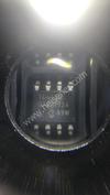
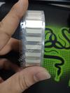
| Part Number | AP139-33WG-7 |
|---|---|
| Manufacturer | Diodes Incorporated |
| Description | IC REG LINEAR 3.3V 300MA SOT25 |
| Datasheet | |
| Package | SC-74A, SOT-753 |
| ECAD |
|
| In Stock | 622,644 piece(s) |
| Unit Price | $ 0.5563 * |
| Lead Time | Can Ship Immediately |
| Estimated Delivery Time | Apr 28 - May 3 (Choose Expedited Shipping) |
| Request for Quotation |
|
| Payment Methods | |
| Delivery Services |
Part Number # AP139-33WG-7 (PMIC - Voltage Regulators - Linear) is manufactured by Diodes Incorporated and distributed by Heisener. Being one of the leading electronics distributors, we carry many kinds of electronic components from some of the world’s top class manufacturers. Their quality is guaranteed by its stringent quality control to meet all required standards.
For AP139-33WG-7 specifications/configurations, quotation, lead time, payment terms of further enquiries please have no hesitation to contact us. To process your RFQ, please add AP139-33WG-7 with quantity into BOM. Heisener.com does NOT require any registration to request a quote of AP139-33WG-7.
| Manufacturer | Diodes Incorporated |
| Category | Integrated Circuits (ICs) - PMIC - Voltage Regulators - Linear |
| Package | SC-74A, SOT-753 |
| ECAD |
|
| Series | - |
| Output Configuration | Positive |
| Output Type | Fixed |
| Number of Regulators | 1 |
| Voltage - Input (Max) | 5.5V |
| Voltage - Output (Min/Fixed) | 3.3V |
| Voltage - Output (Max) | - |
| Voltage Dropout (Max) | 0.45V @ 300mA |
| Current - Output | 300mA |
| Current - Quiescent (Iq) | - |
| Current - Supply (Max) | 60µA |
| PSRR | 75dB ~ 30dB (1KHz ~ 100KHz) |
| Control Features | Enable |
| Protection Features | Over Current, Over Temperature |
| Operating Temperature | -40°C ~ 85°C |
| Mounting Type | Surface Mount |
| Package / Case | SC-74A, SOT-753 |
| Supplier Device Package | SOT-25 |
Izabe*****onway
March 21, 2023
Natha*****ebert
March 19, 2023
Phil*****ennedy
March 14, 2023
Ang*****Lall
March 8, 2023
Tatia*****rtlett
February 28, 2023


|
2225Y0250683KXR | Knowles Syfer, CAP CER 2225, -, - | View |
|
|
39D127F150GL6 | Vishay Sprague, CAP ALUM 120UF 150V AXIAL, Axial, Can, - | View |
|
|
B43508C2827M | EPCOS (TDK), CAP ALUM 820UF 20% 200V SNAP, Radial, Can - Snap-In, - | View |
|
|
AFBR-S10TR001Z | Broadcom Limited, TX FIBER OPTIC POF, -, - | View |

|
PT370012 | TE Connectivity Potter & Brumfield Relays, RELAY GEN PURPOSE 3PDT 10A 12V, -, - | View |

|
Y145322K0000C9L | Vishay Foil Resistors (Division of Vishay Precision Group), RES 22K OHM 0.6W 0.25% RADIAL, Radial, - | View |

|
RT0805CRB07332KL | Yageo, RES SMD 332K OHM 0.25% 1/8W 0805, 0805 (2012 Metric), - | View |

|
801-83-045-10-173101 | Preci-Dip, PCB CONN SOLDER TAIL 2.54MM, -, - | View |

|
SSQ-119-03-G-S | Samtec Inc., CONN RCPT .100" 19POS SNGL GOLD, -, - | View |
|
|
D38999/26MG39JD-LC | Amphenol Aerospace Operations, CONN PLG HSG FMALE 39POS INLINE, -, - | View |
|
|
TPS549B22RVFR | Texas Instruments, TPS549B22RVFR, 40-LFQFN Exposed Pad, - | View |

|
FAN2500S27X | ON Semiconductor, IC REG LINEAR 2.7V 100MA SOT23-5, SC-74A, SOT-753, - | View |

We guarantee 100% customer satisfaction.
Our experienced sales team and tech support team back our services to satisfy all our customers.

We provide 90 days warranty.
If the items you received were not in perfect quality, we would be responsible for your refund or replacement, but the items must be returned in their original condition.
| Part Number | Manufacturer | Description | Stock |
AP139-33WG-7 D# 70550355 |
Diodes Incorporated |
300mA 3.3V Low-Noise LDO Regulator SOT25 RoHS: Not Compliant
|
0 |
| Part Number | Manufacturer | Description | Stock |
AP139-33WG-7 D# V72:2272_06685913 |
Zetex / Diodes Inc |
LDO Regulator Pos 3.3V 0.3A 5-Pin SOT-25 T/R RoHS: Compliant
|
0 |
| Part Number | Manufacturer | Description | Stock |
AP139-33WG-7 D# AP139-33WG-7 |
Diodes Incorporated |
LDO Regulator Pos 3.3V 0.3A 5-Pin SOT-25 T/R - Tape and Reel (Alt: AP139-33WG-7) RoHS: Compliant
|
0 |
| Part Number | Manufacturer | Description | Stock |
AP139-33WG-7 D# AP139-33WG-7 |
Diodes Incorporated |
LDO Regulator Pos 3.3V 0.3A 5-Pin SOT-25 T/R (Alt: AP139-33WG-7) |
0 |
| Part Number | Manufacturer | Description | Stock |
AP139-33WG-7 |
Diodes Incorporated |
300MA 3.3V REGULATOR |
0 |
| Part Number | Manufacturer | Description | Stock |
AP139-33WG-7 D# AP139-33WGCT-ND |
Diodes Incorporated |
IC REG LINEAR 3.3V 300MA SOT25 |
3588 |
| Part Number | Manufacturer | Description | Stock |
AP139-33WG-7 |
VBsemi Electronics Co Ltd |
In stock shipping within 2days |
33525 |
| Part Number | Manufacturer | Description | Stock |
AP139-33WG-7 D# 1825310 |
Diodes Incorporated |
IC, LDO, REG, 3.3V, 300MA, SC59 RoHS: Compliant
Min Qty: 1
Container: Cut Tape
|
0 |
| Part Number | Manufacturer | Description | Stock |
AP139-33WG-7 |
Diodes Incorporated |
AP139 Series 3 V 300 mA Fixed Surface Mount Voltage Regulator - SOT-23 RoHS: Compliant
pbFree: Yes
|
0 |
| Part Number | Manufacturer | Description | Stock |
AP13933WG7 |
DIODES INCORPORATED |
OEM/CM QUOTES ONLY | NO BROKERS |
13800 |
| Part Number | Manufacturer | Description | Stock |
AP13933WG7 |
Analog Devices Inc |
OEM/CM ONLY |
2723 |
| Part Number | Manufacturer | Description | Stock |
AP139-33WG-7 |
Diodes Incorporated |
OEM/CM Immediate delivery |
99000 |
| Part Number | Manufacturer | Description | Stock |
AP139-33WG-7 D# 621-AP139-33WG-7 |
Diodes Incorporated |
LDO Voltage Regulators LDO CMOS 300mA 0.5V MAX VOUT+0.5-7V 3.3V RoHS: Compliant
|
4073 |
| Part Number | Manufacturer | Description | Stock |
AP139-33WG-7 D# NS-AP139-33WG-7 |
Diodes Incorporated |
OEM/CM ONLY |
8812 |
| Part Number | Manufacturer | Description | Stock |
AP139-33WG-7 D# 8228795P |
Zetex / Diodes Inc |
DiodesZetex AP139-33WG-7, LDO Regulator, 300mA, 3.3 V, 2% 5-Pin, SOT-25, RL Min Qty: 20
Container: Reel
|
2520 |
| Part Number | Manufacturer | Description | Stock |
AP13933WG7 |
Diodes Incorporated |
OEM/CM ONLY |
3016 |
| Part Number | Manufacturer | Description | Stock |
AP139-33WG-7 |
Diodes Incorporated |
IN stock Immediate delivery |
98985 |
| Part Number | Manufacturer | Description | Stock |
AP139-33WG-7 |
Diodes Incorporated |
shipping today |
2002 |
| Part Number | Manufacturer | Description | Stock |
AP139-33WG-7 D# 26749063 |
Zetex / Diodes Inc |
LDO Regulator Pos 3.3V 0.3A 5-Pin SOT-25 T/R RoHS: Compliant
|
0 |
| Part Number | Manufacturer | Description | Stock |
AP139-33WG-7 |
Diodes Incorporated |
RFQ |
5569 |
| Part Number | Manufacturer | Description | Stock |
AP139-33WG-7 |
Diodes Incorporated |
IC REG LDO 3.3V 0.3A SOT25 |
8976 |
Heisener's commitment to quality has shaped our processes for sourcing, testing, shipping, and every step in between. This foundation underlies each component we sell.

Do you have any question about AP139-33WG-7?
+86-755-83210559 ext. 815


Scan to view this page