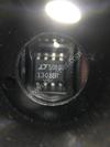
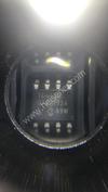
| Part Number | DS1267BE-010+ |
|---|---|
| Manufacturer | Maxim Integrated |
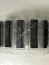
| Description | IC DGTL POT 10K 2CH 20TSSOP |
| Datasheet | |
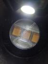
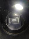
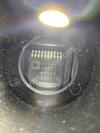
| Package | 20-TSSOP (0.173", 4.40mm Width) |
| ECAD |
|
| In Stock | 4,560 piece(s) |
| Unit Price | $ 8.8753 * |
| Lead Time | Can Ship Immediately |
| Estimated Delivery Time | Apr 28 - May 3 (Choose Expedited Shipping) |
| Request for Quotation |
|
| Payment Methods | |
| Delivery Services |
Part Number # DS1267BE-010+ (Data Acquisition - Digital Potentiometers) is manufactured by Maxim Integrated and distributed by Heisener. Being one of the leading electronics distributors, we carry many kinds of electronic components from some of the world’s top class manufacturers. Their quality is guaranteed by its stringent quality control to meet all required standards.
For DS1267BE-010+ specifications/configurations, quotation, lead time, payment terms of further enquiries please have no hesitation to contact us. To process your RFQ, please add DS1267BE-010+ with quantity into BOM. Heisener.com does NOT require any registration to request a quote of DS1267BE-010+.
| Manufacturer | Maxim Integrated |
| Category | Integrated Circuits (ICs) - Data Acquisition - Digital Potentiometers |
| Package | 20-TSSOP (0.173", 4.40mm Width) |
| ECAD |
|
| Series | - |
| Taper | Linear |
| Configuration | Potentiometer |
| Number of Circuits | 2 |
| Number of Taps | 256 |
| Resistance (Ohms) | 10k |
| Interface | Serial |
| Memory Type | Volatile |
| Voltage - Supply | 5V |
| Features | Cascade Pin |
| Tolerance | ±20% |
| Temperature Coefficient (Typ) | 750 ppm/°C |
| Resistance - Wiper (Ohms) (Typ) | 900 |
| Operating Temperature | -40°C ~ 85°C |
| Package / Case | 20-TSSOP (0.173", 4.40mm Width) |
| Supplier Device Package | 20-TSSOP |
Brans*****rghese
April 6, 2023
Trey*****dman
March 29, 2023
Ann*****ass
March 21, 2023
Yisro*****afford
March 11, 2023
Chris*****r Samra
March 11, 2023
Die*****Soto
March 11, 2023
Lawr***** Mills
March 5, 2023
Jozi*****arin
February 25, 2023


|
1206J0160391MDT | Knowles Syfer, CAP CER 390PF 16V X7R 1206, 1206 (3216 Metric), - | View |

|
HAU220KBACD0KR | Vishay BC Components, CAP CER 22PF 1KV N750 RADIAL, Radial, Disc, - | View |
|
|
B43501B5397M87 | EPCOS (TDK), CAP ALUM 390UF 20% 450V SNAP, Radial, Can - Snap-In, - | View |
 
|
25AA256T-I/SN | Microchip Technology, IC EEPROM 256KBIT 10MHZ 8SOIC, 8-SOIC (0.154", 3.90mm Width), - | View |

|
SMF40A-E3-18 | Vishay Semiconductor Diodes Division, TVS DIODE 40VWM 64.5VC DO-219AB, DO-219AB, - | View |
|
|
PDB-708-SMA | Luna Optoelectronics, PHOTODIODE FIBER OPTIC SMA CONN, TO-18-6, - | View |
|
|
OV09728-A30A | OmniVision Technologies Inc, IC IMAGE SENSOR 720P 40-CSP3, Module, - | View |
|
|
CMF651K0000FKEA11 | Vishay Dale, RES 1K OHM 1.5W 1% AXIAL, Axial, - | View |

|
RT1206BRC071K54L | Yageo, RES SMD 1.54K OHM 0.1% 1/4W 1206, 1206 (3216 Metric), - | View |

|
RT0805DRD07464KL | Yageo, RES SMD 464K OHM 0.5% 1/8W 0805, 0805 (2012 Metric), - | View |
|
|
EJH-125-01-F-D-SM-LC-05-K | Samtec Inc., .100 X .100 EJECTOR HEADER ASSEM, -, - | View |

|
MDP-4# | Pomona Electronics, PLUG DBL BANANA W/WIRE GUIDE YEL, -, - | View |

We guarantee 100% customer satisfaction.
Our experienced sales team and tech support team back our services to satisfy all our customers.

We provide 90 days warranty.
If the items you received were not in perfect quality, we would be responsible for your refund or replacement, but the items must be returned in their original condition.
| Part Number | Manufacturer | Description | Stock |
DS1267BE-010+ D# DS1267BE-010+ |
Maxim Integrated Products |
Digital Potentiometer 256POS 10k Ohm 2Pot 20-Pin TSSOP Tube - Rail/Tube (Alt: DS1267BE-010+) |
0 |
DS1267BE-010+T/R D# DS1267BE-010+T/R |
Maxim Integrated Products |
Digital Potentiometer 256POS 10k Ohm 2Pot 20-Pin TSSOP T/R - Tape and Reel (Alt: DS1267BE-010+T/R) |
0 |
| Part Number | Manufacturer | Description | Stock |
DS1267BE-010+ D# DS1267BE-010+ |
Maxim Integrated Products |
Digital Potentiometer 256POS 10k Ohm 2Pot 20-Pin TSSOP Tube (Alt: DS1267BE-010+) |
0 |
DS1267BE-010+T/R D# DS1267BE-010+T/R |
Maxim Integrated Products |
Digital Potentiometer 256POS 10k Ohm 2Pot 20-Pin TSSOP T/R (Alt: DS1267BE-010+T/R) |
0 |
| Part Number | Manufacturer | Description | Stock |
DS1267BE-010+T/R |
Maxim Integrated Products |
DUAL 256-STEP DIGITAL POTENTIOMETER - Tape and Reel |
0 |
DS1267BE-010+ |
Maxim Integrated Products |
DUAL 256-STEP DIGITAL POTENTIOMETER - Tape and Reel |
0 |
| Part Number | Manufacturer | Description | Stock |
DS1267BE-010+ |
Maxim Integrated Products |
RoHS (ship within 1day) - D/C 2016 |
89 |
| Part Number | Manufacturer | Description | Stock |
DS1267BE-010+T/R D# DS1267BE-010+T/R-ND |
Maxim Integrated Products |
IC DGT POT 10KOHM 256TAP 20TSSOP |
0 |
DS1267BE-010+ D# DS1267BE-010+-ND |
Maxim Integrated Products |
IC DGT POT 10KOHM 256TAP 20TSSOP |
233 |
| Part Number | Manufacturer | Description | Stock |
DS1267BE-010+ D# 2515862 |
Maxim Integrated Products |
DIGITAL POT, 10K, DUAL, TSSOP-20 RoHS: Compliant
Min Qty: 1
Container: Each
|
52 |
| Part Number | Manufacturer | Description | Stock |
DS1267BE-010+ |
Maxim Integrated Products |
Dual 256-step digital potentiometer RoHS: Compliant
pbFree: Yes
|
0 |
DS1267BE-010+T/R |
Maxim Integrated Products |
Dual 256-step digital potentiometer RoHS: Compliant
pbFree: Yes
|
0 |
| Part Number | Manufacturer | Description | Stock |
DS1267BE010 |
MAXIM INTEGRATED PRODUCTS |
OEM/CM QUOTES ONLY | NO BROKERS |
170 |
| Part Number | Manufacturer | Description | Stock |
DS1267BE010 |
Maxim Integrated Products |
OEM/CM ONLY |
441 |
DS1267BE010TR |
Maxim Integrated Products |
OEM/CM ONLY |
442 |
| Part Number | Manufacturer | Description | Stock |
DS1267BE-010+ D# 700-DS1267BE-010+ |
Maxim Integrated Products |
Digital Potentiometer ICs Dual 256-step digital potentiometer RoHS: Compliant
|
61 |
| Part Number | Manufacturer | Description | Stock |
DS1267BE-010+ D# 73Y1185 |
Maxim Integrated Products |
DIGITAL POT, 10K, DUAL, TSSOP-20, End To End Resistance:10kohm, No. of Pots:Dual, Control Interface:SPI, Track Taper:Linear, Resistance Tolerance:± 20%, Supply Voltage Min:4.5V, Supply Voltage Max:5.5V, No. of Pins:20Pins RoHS Compliant: Yes RoHS: Compliant
Min Qty: 1
Container: Bulk
|
52 |
| Part Number | Manufacturer | Description | Stock |
DS1267BE-010+ |
Maxim Integrated Products | 71 |
| Part Number | Manufacturer | Description | Stock |
DS1267BE-010+ D# 1904759 |
Maxim Integrated Products |
DS1267BE-010+, Digital Potentiometer 10k 256-Position Linear 2-Channel Serial-3 Wire 20 Pin, TSSOP, TU Min Qty: 74
Container: Tube
|
442 |
| Part Number | Manufacturer | Description | Stock |
DS1267BE010+T/R |
Maxim Integrated Products |
OEM/CM ONLY |
2595 |
DS1267BE010+ |
Maxim Integrated Products |
OEM/CM ONLY |
105 |
| Part Number | Manufacturer | Description | Stock |
DS1267BE-010+T/R |
Maxim Integrated Products |
RFQ |
9941 |
| Part Number | Manufacturer | Description | Stock |
DS1267BE-010+ D# 2515862 |
Maxim Integrated Products |
DIGITAL POT, 10K, DUAL, TSSOP-20 RoHS: Compliant
Min Qty: 1
Container: Each
|
52 |
Heisener's commitment to quality has shaped our processes for sourcing, testing, shipping, and every step in between. This foundation underlies each component we sell.

Do you have any question about DS1267BE-010+?
+86-755-83210559 ext. 805


Scan to view this page