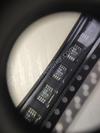
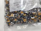
Part Number | MOC3010SVM |
---|---|
Manufacturer | Fairchild/ON Semiconductor |
Description | OPTOISOLATOR 4.17KV TRIAC 6SMD |
Datasheet | MOC3010SVM Datasheet |
Package | 6-SMD, Gull Wing |
In Stock | 4,000 piece(s) |
Unit Price | Request a Quote |
Lead Time | Can Ship Immediately |
Estimated Delivery Time | Jan 30 - Feb 4 (Choose Expedited Shipping) |
Request for Quotation |
|
Part Number # MOC3010SVM (Optoisolators - Triac, SCR Output) is manufactured by Fairchild/ON Semiconductor and distributed by Heisener. Being one of the leading electronics distributors, we carry many kinds of electronic components from some of the world’s top class manufacturers. Their quality is guaranteed by its stringent quality control to meet all required standards.
For MOC3010SVM specifications/configurations, quotation, lead time, payment terms of further enquiries please have no hesitation to contact us. To process your RFQ, please add MOC3010SVM with quantity into BOM. Heisener.com does NOT require any registration to request a quote of MOC3010SVM.
Manufacturer | Fairchild/ON Semiconductor |
Category | Isolators - Optoisolators - Triac, SCR Output |
Datasheet | MOC3010SVMDatasheet |
Package | 6-SMD, Gull Wing |
Series | - |
Output Type | Triac |
Zero Crossing Circuit | No |
Number of Channels | 1 |
Voltage - Isolation | 4170Vrms |
Voltage - Off State | 250V |
Static dV/dt (Min) | - |
Current - LED Trigger (Ift) (Max) | 15mA |
Current - On State (It (RMS)) (Max) | - |
Current - Hold (Ih) | 100µA (Typ) |
Turn On Time | - |
Voltage - Forward (Vf) (Typ) | 1.15V |
Current - DC Forward (If) (Max) | 60mA |
Operating Temperature | -40°C ~ 85°C |
Mounting Type | Surface Mount |
Package / Case | 6-SMD, Gull Wing |
Supplier Device Package | 6-SMD |
Approvals | IEC/EN/DIN, UL |
To learn more about ON Semiconductor, please visit our website at www.onsemi.com Please note: As part of the Fairchild Semiconductor integration, some of the Fairchild orderable part numbers will need to change in order to meet ON Semiconductor’s system requirements. Since the ON Semiconductor product management systems do not have the ability to manage part nomenclature that utilizes an underscore (_), the underscore (_) in the Fairchild part numbers will be changed to a dash (-). This document may contain device numbers with an underscore (_). Please check the ON Semiconductor website to verify the updated device numbers. The most current and up-to-date ordering information can be found at www.onsemi.com. Please email any questions regarding the system integration to Fairchild_questions@onsemi.com. Is Now Part of ON Semiconductor and the ON Semiconductor logo are trademarks of Semiconductor Components Industries, LLC dba ON Semiconductor or its subsidiaries in the United States and/or other countries. ON Semiconductor owns the rights to a number of patents, trademarks, copyrights, trade secrets, and other intellectual property. A listing of ON Semiconductor’s product/patent coverage may be accessed at www.onsemi.com/site/pdf/Patent-Marking.pdf. ON Semiconductor reserves the right to make changes without further notice to any products herein. ON Semiconductor makes no warranty, representation or guarantee regarding the suitability of its products for any particular purpose, nor does ON Semiconductor assume any liability arising out of the application or use of any product or circuit, and specifically disclaims any and all liability, including without limitation special, consequential or incidental damages. Buyer is responsible for its products and applications using ON Semiconductor products, including compliance with all laws, regulations and safety requirements or standards, regardless of any support or applications information provided by ON Semiconductor. “Typical” parameters which may be provided in ON Semiconductor data sheets and/or specifications can and do vary in different applications and actual performance may vary over time. All operating parameters, including “Typicals” must be validated for each customer application by customer’s technical experts. ON Semiconductor does not convey any license under its patent rights nor the rights of others. ON Semiconductor products are not designed, intended, or authorized for use as a critical component in life support systems or any FDA Class 3 medical devices or medical devices with a same or similar classification in a foreign jurisdiction or any devices intended for implantation in the human body. Should Buyer purchase or use ON Semiconductor products for any such unintended or unauthorized application, Buyer shall indemnify and hold ON Semiconductor and its officers, employees, subsidiaries, affiliates, and distributors harmless against all claims, costs, damages, and expenses, and reasonable attorney fees arising out of, directly or indirectly, any claim of personal injury or death associated with such unintended or unauthorized use, even if such claim alleges that ON Semiconductor was negligent regarding the design or manufacture of the part. ON Semiconductor is an Equal Opportunity/Affirmative Action Employer. This literature is subject to all applicable copyright laws and is not for resale in any manner.
M O C 301X M , M O C 302X M — 6-P in D IP R a n d o m -P h ase Triac D river O u tp u t O p to co u p ler (250/400 V o lt P eak) ©2005 Fairchild Semiconductor Corporation www.fairchildsemi.com MOC301XM, MOC302XM Rev. 1.5 July 2015 MOC3010M, MOC3011M, MOC3012M, MOC3020M, MOC3021M, MOC3022M, MOC3023M 6-Pin DIP Random-Phase Triac Driver Output Optocoupler (250/400 Volt Peak) Features • Excellent IFT Stability—IR Emitting Diode Has Low Degradation • Peak Blocking Voltage – 250 V, MOC301XM – 400 V, MOC302XM • Safety and Regulatory Approvals – UL1577, 4,170 VACRMS for 1 Minute – DIN EN/IEC60747-5-5 Applications • Industrial Controls • Solenoid/Valve Controls • Traffic Lights • Static AC Power Switch • Vending Machines • Incandescent Lamp Dimmers • Solid State Relay • Motor Control • Lamp Ballasts Description The MOC301XM and MOC302XM series are optically isolated triac driver devices. These devices contain a GaAs infrared emitting diode and a light activated silicon bilateral switch, which functions like a triac. They are designed for interfacing between electronic controls and power triacs to control resistive and inductive loads for 115 VAC operations. Schematic Package Outlines Figure 1. Schematic Figure 2. Package Outlines MAIN TERM. NC* N/C *DO NOT CONNECT (TRIAC SUBSTRATE) 1 2 3 ANODE CATHODE 4 5 6 MAIN TERM.
©2005 Fairchild Semiconductor Corporation www.fairchildsemi.com MOC301XM, MOC302XM Rev. 1.5 2 M O C 301X M , M O C 302X M — 6-P in D IP R a n d o m -P h ase Triac D river O u tp u t O p to co u p ler (250/400 V o lt P eak) Safety and Insulation Ratings As per DIN EN/IEC 60747-5-5, this optocoupler is suitable for “safe electrical insulation” only within the safety limit data. Compliance with the safety ratings shall be ensured by means of protective circuits. Parameter Characteristics Installation Classifications per DIN VDE 0110/1.89 Table 1, For Rated Mains Voltage < 150 VRMS I–IV < 300 VRMS I–IV Climatic Classification 40/85/21 Pollution Degree (DIN VDE 0110/1.89) 2 Comparative Tracking Index 175 Symbol Parameter Value Unit VPR Input-to-Output Test Voltage, Method A, VIORM x 1.6 = VPR, Type and Sample Test with tm = 10 s, Partial Discharge < 5 pC 1275 Vpeak Input-to-Output Test Voltage, Method B, VIORM x 1.875 = VPR, 100% Production Test with tm = 1 s, Partial Discharge < 5 pC 1594 Vpeak VIORM Maximum Working Insulation Voltage 850 Vpeak VIOTM Highest Allowable Over-Voltage 6000 Vpeak External Creepage ≥ 7 mm External Clearance ≥ 7 mm External Clearance (for Option TV, 0.4" Lead Spacing) ≥ 10 mm DTI Distance Through Insulation (Insulation Thickness) ≥ 0.5 mm RIO Insulation Resistance at TS, VIO = 500 V > 10 9 Ω
©2005 Fairchild Semiconductor Corporation www.fairchildsemi.com MOC301XM, MOC302XM Rev. 1.5 3 M O C 301X M , M O C 302X M — 6-P in D IP R a n d o m -P h ase Triac D river O u tp u t O p to co u p ler (250/400 V o lt P eak) Absolute Maximum Ratings Stresses exceeding the absolute maximum ratings may damage the device. The device may not function or be operable above the recommended operating conditions and stressing the parts to these levels is not recommended. In addition, extended exposure to stresses above the recommended operating conditions may affect device reliability. The absolute maximum ratings are stress ratings only. TA = 25°C unless otherwise specified. Symbol Parameters Device Value Unit TOTAL DEVICE TSTG Storage Temperature All -40 to +150 °C TOPR Operating Temperature All -40 to +85 °C TJ Junction Temperature Range All -40 to +100 °C TSOL Lead Solder Temperature All 260 for 10 seconds °C PD Total Device Power Dissipation at 25°C Ambient All 330 mW Derate Above 25°C 4.4 mW/°C EMITTER IF Continuous Forward Current All 60 mA VR Reverse Voltage All 3 V PD Total Power Dissipation at 25°C Ambient All 100 mW Derate Above 25°C 1.33 mW/°C DETECTOR VDRM Off-State Output Terminal Voltage MOC3010M MOC3011M MOC3012M 250 VMOC3020M MOC3021M MOC3022M MOC3023M 400 ITSM Peak Repetitive Surge Current (PW = 100 μs, 120 pps) All 1 A PD Total Power Dissipation at 25°C Ambient All 300 mW Derate Above 25°C 4 mW/°C
©2005 Fairchild Semiconductor Corporation www.fairchildsemi.com MOC301XM, MOC302XM Rev. 1.5 4 M O C 301X M , M O C 302X M — 6-P in D IP R a n d o m -P h ase Triac D river O u tp u t O p to co u p ler (250/400 V o lt P eak) Electrical Characteristics TA = 25°C unless otherwise specified. Individual Component Characteristics Transfer Characteristics Isolation Characteristics Notes: 1. Test voltage must be applied within dv/dt rating. 2. All devices are guaranteed to trigger at an IF value less than or equal to max IFT. Therefore, recommended operating IF lies between max IFT (30 mA for MOC3020M, 15 mA for MOC3010M and MOC3021M, 10 mA for MOC3011M and MOC3022M, 5 mA for MOC3012M and MOC3023M) and absolute maximum IF (60 mA). 3. Isolation voltage, VISO, is an internal device dielectric breakdown rating. For this test, pins 1 and 2 are common, and pins 4, 5 and 6 are common. Symbol Parameters Test Conditions Device Min. Typ. Max. Unit EMITTER VF Input Forward Voltage IF = 10 mA All 1.15 1.50 V IR Reverse Leakage Current VR = 3 V, TA = 25°C All 0.01 100 μA DETECTOR IDRM Peak Blocking Current, Either Direction Rated VDRM, IF = 0 (1) All 10 100 nA VTM Peak On-State Voltage, Either Direction ITM = 100 mA peak, IF = 0 All 1.8 3.0 V Symbol DC Characteristics Test Conditions Device Min. Typ. Max. Unit IFT LED Trigger Current Voltage = 3 V (2) MOC3020M 30 mA MOC3010M 15 MOC3021M MOC3011M 10 MOC3022M MOC3012M 5 MOC3023M IH Holding Current, Either Direction All 100 μA Symbol Parameter Test Conditions Device Min. Typ. Max. Unit VISO Isolation Voltage (3) t = 1 Minute All 4170 VACRMS
©2005 Fairchild Semiconductor Corporation www.fairchildsemi.com MOC301XM, MOC302XM Rev. 1.5 5 M O C 301X M , M O C 302X M — 6-P in D IP R a n d o m -P h ase Triac D river O u tp u t O p to co u p ler (250/400 V o lt P eak) Typical Performance Curves AMBIENT TEMPERATURE - T A ( o C) -40 -20 0 20 40 60 80 100 I T M - T R IG G E R C U R R E N T ( N O R M A L IZ E D ) 0.6 0.7 0.8 0.9 1.0 1.1 1.2 1.3 1.4 I F - LED FORWARD CURRENT (mA) 1 10 100 V F - F O R W A R D V O L T A G E ( V ) 1.0 1.1 1.2 1.3 1.4 1.5 1.6 1.7 1.8 TA = -55 o C TA = 25 o C TA = 100 o C VTM - ON-STATE VOLTAGE (V) -3 -2 -1 0 1 2 3 I T M - O N -S T A T E C U R R E N T ( m A ) -800 -600 -400 -200 0 200 400 600 800 TA - AMBIENT TEMPERATURE ( o C) TA - AMBIENT TEMPERATURE ( o C) -40 -20 0 20 40 60 80 100 I D R M - L E A K A G E C U R R E N T ( n A ) 0.1 1 10 100 1000 10000 NORMALIZED TO TA = 25°C Figure 3. LED Forward Voltage vs. Forward Current Figure 5. Trigger Current vs. Ambient Temperature PWin - LED TRIGGER WIDTH (μs) 1 2 5 10 20 50 100 I F T - T R IG G E R C U R R E N T ( N O R M A L IZ E D ) 0 5 10 15 20 25 NORMALIZED TO: PWin ≥ 100 μs Figure 6. LED Current Required to Trigger vs. LED Pulse Width Figure 8. Leakage Current, IDRM vs. Temperature Figure 4. On-State Characteristics 25 30 40 6050 70 80 90 100 S T A T IC d v /d t (V /μ s ) 0 2 4 6 8 10 12 STATIC dv/dt CIRCUIT IN FIGURE 9 Figure 7. dv/dt vs. Temperature
©2005 Fairchild Semiconductor Corporation www.fairchildsemi.com MOC301XM, MOC302XM Rev. 1.5 6 M O C 301X M , M O C 302X M — 6-P in D IP R a n d o m -P h ase Triac D river O u tp u t O p to co u p ler (250/400 V o lt P eak) Note: This optoisolator should not be used to drive a load directly. It is intended to be a trigger device only. Figure 9. Static dv/dt Test Circuit Figure 10. Resistive Load Figure 11. Inductive Load with Sensitive Gate Triac (IGT ≤ 15 mA) Vdc 400 V (MOC302X) 250 V (MOC301X) R = 10 kΩ CTEST X100 SCOPE PROBE PULSE INPUT MERCURY WETTED RELAY RTEST DUT 252 V (MOC302X) 158 V (MOC301X) 0 VOLTS APPLIED VOLTAGE WAVEFORM Vmax = dv/dt = 0.63 Vmax = 252 RC RC RC 400 V (MOC302X) = 250 V (MOC301X) (MOC302X) = 158 RC (MOC301X) 1. The mercury wetted relay provides a high speed repeated pulse to the D.U.T. 2. 100x scope probes are used, to allow high speeds and voltages. 3. The worst-case condition for static dv/dt is established by triggering the DUT with a normal LED input current, then removing the current. The variable RTEST allows the dv/dt to be gradually increased until the DUT continues to trigger in response to the applied voltage pulse, even after the LED current has been removed. The dv/dt is then decreased until the DUT stops triggering. τRC is measured at this point and recorded. VCC Rin 1 2 3 6 5 4 120 V 60 Hz 180 Ω RL MOC3010M MOC3011M MOC3012M VCC Rin 1 2 3 6 5 4 0.1 μF 180 Ω C1 2.4 kΩ ZL 120 V 60 HzMOC3010M MOC3011M MOC3012M
©2005 Fairchild Semiconductor Corporation www.fairchildsemi.com MOC301XM, MOC302XM Rev. 1.5 7 M O C 301X M , M O C 302X M — 6-P in D IP R a n d o m -P h ase Triac D river O u tp u t O p to co u p ler (250/400 V o lt P eak) Figure 12. Inductive Load with sensitive Gate Triac (IGT ≤ 15 mA) Figure 13. Typical Application Circuit Rin VCC 1 2 3 6 5 4 0.2 μF 180 Ω C1 1.2 kΩ ZL 120 V 60 HzMOC3010M MOC3011M MOC3012M VCC Rin 1 2 3 6 5 4 0.05 μF 0.01 μF LOAD 360 Ω 39 470 Ω 240 VAC HOT GROUND MOC3020M MOC3021M MOC3022M MOC3023M In this circuit the “hot” side of the line is switched and the load connected to the cold or ground side. The 39 Ω resistor and 0.01 μF capacitor are for snubbing of the triac, and the 470 Ω resistor and 0.05 μF capacitor are for snubbing the coupler. These components may or may not be necessary depending upon the particular and load used.
©2005 Fairchild Semiconductor Corporation www.fairchildsemi.com MOC301XM, MOC302XM Rev. 1.5 8 M O C 301X M , M O C 302X M — 6-P in D IP R a n d o m -P h ase Triac D river O u tp u t O p to co u p ler (250/400 V o lt P eak) Reflow Profile Figure 14. Reflow Profile 300 280 260 240 220 200 180 160 140 120 100 80 60 40 20 0 °C Time (s) 0 60 180120 270 260°C >245°C = 42 s Time Above 183°C = 90 s 360 1.822°C/s Ramp-up Rate 33 s
Elia*****arvey
December 4, 2020
For*****ouse
December 3, 2020
Oli***** Hall
November 25, 2020
Abdie*****haria
November 23, 2020
Mar***** Dada
November 19, 2020
We guarantee 100% customer satisfaction.
Our experienced sales team and tech support team back our services to satisfy all our customers.
We provide 90 days warranty.
If the items you received were not in perfect quality, we would be responsible for your refund or replacement, but the items must be returned in their original condition.
Payment Methods | |
Delivery Services |
Heisener's commitment to quality has shaped our processes for sourcing, testing, shipping, and every step in between. This foundation underlies each component we sell.