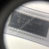
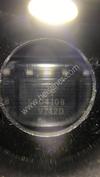
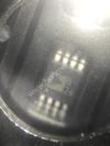
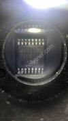
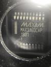
Page 1
Page 2
1/15
STA120
December 2002
■ MONOLITHIC CMOS RECEIVER
■ 3.3V SUPPLY VOLTAGE
■ LOW-JITTER, ON-CHIP CLOCK RECOVERY
256xFs OUTPUT CLOCK PROVIDED
■ SUPPORTS: AES/EBU, IEC 958, S/PDIF, &
EIAJ CP-340/1201 PROFESSIONAL AND
CONSUMER FORMATS
■ EXTENSIVE ERROR REPORTING REPEAT
LAST SAMPLE ON ERROR OPTION
DESCRIPTION
The STA120 is a monolithic CMOS device that re-
ceives and decodes audio data according to the
AES/EBU, IEC 958, S/PDIF, & EIAJ CP-340/1201
interface standards.
The STA120 recovers the clock and synchroniza-
tion signals and de-multiplexes the audio and dig-
ital data. Differential or single ended inputs can be
decoded.
The STA120 de-multiplexes the channel, user and
validity data directly to serial output pins with ded-
icated output pins for the most important channel
status bits.
SO28
ORDERING NUMBER: STA120D
DIGITAL AUDIO INTERFACE RECEIVER
BLOCK DIAGRAM
AUDIO
SERIAL PORT
REGISTERS
DE MUX
CLOCK & DATA
RECOVERY
C0/E0
M2 M0AGNDFILT
SDATA
SCK
FSYNC
C
U
VREF
ERF CBL
RXP
9
25 15
26
12
11
2318
6
1
14
28
D97AU613A
M1
24
VA+ MCK
87
DGNDVD+
19212022
RS422
Receiver
RXN
10
MUX
13
CS12/FCK
16
SEL
MUX
Ca/E1
5
Cb/E2
4
Cc/F0
3
Cd/F1
2
Ce/F2
27
M3
17
Page 3
STA120
2/15
ABSOLUTE MAXIMUM RATINGS
PIN CONNECTIONS (Top view)
Symbol Parameter Value Unit
VD+, VA+ Power Supply Voltage 4 V
VIN Input Voltage ( excluding pins 9, 10) -0.3 to VD+ +0.3 V
Tamb Ambient Operating Temperature (power applied) -30 to +85 °C
Tstg Storage Temperature -40 to 150 °C
PINS DESCRIPTION
N. Name Description
Power Supply
7 VD+ Positive Digital Power.Positive supply for the digital section. Nominally 3.3V.
8 DGND Digital Ground.Ground for the digital section.
21 AGND Analog Ground.Ground for the analog section. AGND should be connected to same ground as
DGND.
22 VA+ Positive Analog Power.Positive supply for the analog section. Nominally 3.3V.
Audio Output Interface
11 FSYNC Frame Sync.Delineates the serial data and may indicate the particular channel, left or right and
may be an input or output. The format is based on M0, M1, M2 and M3 pins.
12 SCK Serial Clock.Serial clock for SDATA pin which can be configured (via the M0, M1, M2 and M3
pins) as an input or output and can sample data on the rising or falling edge. As an output, SCK
will generate 32 clocks for every audio sample. As an input, 32 SCK periods per audio sample
must be provided in all normal modes.
17, 18,
23, 24
M2, M3,
M1, M0
Serial Port Mode Selects.Selects the format of Fsync and the sample edge of SCK with respect
to SDATA.
26 SDATA Serial Data. Audio data serial output pin.
C0/E0
VD+
DGND
RXP
RXN
SCK
FSYNC
CS12/FCK
U
1
3
2
4
5
6
7
8
9
CBL
SEL
M3
MCK
M2
FILT
AGND
VA+
M023
22
21
20
19
17
18
16
15
D97AU609A
10
11
12
13
14
28
27
26
25
24
C
Cd/F1
Cc/F0
Cb/E2
Ca/E1 M1
ERF
SDATA
Ce/F2
VERF
Page 4
3/15
STA120
Control Pins
1 C Channel Status Output. Received channel status bit serial output port. FSYNC may be used to
latch this bit externally. Except in I2S modes when this pin is updated at the active edge off
Fsync.
2 Cd Channel Status Output Bits.These pin are dual Function with the "C" bits selected when SEL is
high. Channel status information is displayed for the channel selected by CS12. C0, which is
channel status bit 0, defines professional (C0 = 0) or consumer (C0 = 1) mode and further
controls the definition of the Ca-Ce pins. These pins are updated with the rising edge of CBL.
F1 Frequency reporting Bits.Encoder sample frequency information that is enabled by bringing SEL
low. A proper clock on FCK must be input for at least two thirds of a channel status block for
these pins to be valid. They are updated three times per block, starting at the block boundary.
3 Cc Channel Status Output Bits.These pin are dual Function with the "C" bits selected when SEL is
high. Channel status information is displayed for the channel selected by CS12. C0, which is
channel status bit 0, defines professional (C0 = 0) or consumer (C0 = 1) mode and further
controls the definition of the Ca-Ce pins. These pins are updated with the rising edge of CBL.
F0 Frequency reporting Bits.Encoded sample frequency information that is enabled by bringing SEL
low. A proper clock on FCK must be input for at least two thirds of a channel status block for
these pins to be valid. They are updated three times per block, starting at the block boundary.
4 Cb Channel Status Output Bits.These pin are dual Function with the "C" bits selected when SEL is
high. Channel status information is displayed for the channel selected by CS12. C0, which is
channel status bit 0, defines professional (C0 = 0) or consumer (C0 = 1) mode and further
controls the definition of the Ca-Ce pins. These pins are updated with the rising edge of CBL.
E2 Error Condition.Encoded error information that is enabled by bringing SEL low. The error codes
are prioritized and latched so that the error code displayed is the highest level of error since the
last clearing of the error pins. Clearing is accomplished by bringing SEL high for more than 8
MCK cycles.
5 Ca Channel Status Output Bits.These pin are dual Function with the "C" bits selected when SEL is
high. Channel status information is displayed for the channel selected by CS12. C0, which is
channel status bit 0, defines professional (C0 = 0) or consumer (C0 = 1) mode and further
controls the definition of the Ca-Ce pins. These pins are updated with the rising edge of CBL.
5 E2 Error Condition.Encoded error information that is enabled by bringing SEL low. The error codes
are prioritized and latched so that the error code displayed is the highest level of error since the
last clearing of the error pins. Clearing is accomplished by bringing SEL high for more than 8
MCK cycles.
6 C0 Channel Status Output Bits.These pin are dual Function with the "C" bits selected when SEL is
high. Channel status information is displayed for the channel selected by CS12. C0, which is
channel status bit 0, defines professional (C0 = 0) or consumer (C0 = 1) mode and further
controls the definition of the Ca-Ce pins. These pins are updated with the rising edge of CBL.
E0 Error Condition.Encoded error information that is enabled by bringing SEL low. The error codes
are prioritized and latched so that the error code displayed is the highest level of error since the
last clearing of the error pins. Clearing is accomplished by bringing SEL high for more than 8
MCK cycles.
13 CS12 Channel Select.This pin is also dual function and is selected by bringing SEL high. CS12 selects
sub-frame1 (when low) or sub-frame2 (when high) to be displayed by channel status pins C0 an
Ca through Ce.
FCK Frequency Clock.Frequency Clock input that is enabled by bringing SEL low. FCK is compared to
the received clock frequency with the value displayed on F2 through F0. Nominal input value is
6.144MHz.
14 U User Bit.Received user bit serial output port, FSYNC may be used to latch this bit externally.
Except in I2S modes when this pin is updated at the active edge off Fsync.
15 CBL Channel Status Block Start.The channel status block output is high for the first four bytes of
channel status and low for the last 20 bytes.
PINS DESCRIPTION (continued)
N. Name Description
Page 5
STA120
4/15
DIGITAL CHARACTERISTICS (Tamb = 25°C; VD+, VA+ = 3.3V ±10%)
Note 1: FS is defined as the incoming audio sample frequency per channel.
SWITCHING CHARACTERISTICS - SERIAL PORTS (Tamb = 25°C; VD+, VA+ = 3.3V ±10%)
Note 2: The output word rate, OWR, refers to the frequency at which an audio sample is output from the part. (A stereo pair is two audio
samples). Therefore, in Master mode, there are always 32 SCK periods in one audio sample. In Slave mode 32 SCK periods must
be provided in most serial port formats.
16 SEL Select.Control pin that selects either channel status information (SEL = 1) or error and frequency
information (SEL = 0) to be displayed on six (C0, Ca Cb, Cc, Cd, Ce) pins.
27 Ce Channel Status Output Bits.These pin are dual Function with the "C" bits selected when SEL is
high. Channel status information is displayed for the channel selected by CS12. C0, which is
channel status bit 0, defines professional (C0 = 0) or consumer (C0 = 1) mode and further
controls the definition of the Ca-Ce pins. These pins are updated with the rising edge of CBL.
F2 Frequency reporting Bits.Encoded sample frequency information that is enabled by bringing SEL
low. A proper clock on FCK must be input for at least two thirds of a channel status block for
these pins to be valid. They are updated three times per block, starting at the block boundary.
28 VERF Validity + Error Flag. A logical OR'ing of the validity bit from the received data and the error flag.
May be used by interpolation filters to interpolate through errors.
Receiver Interface
9 RXP Line Receiver. (RS422 compatible)
10 RXN Line Receiver. (RS422 compatible)
Phase Locked Loop
19 MCK Master Clock.Low Jitter clock output of 256 times the received sample frequency.
20 FILT Filter.An external 330 Ohm resistor and 0.47µF capacitor in parallel with a 15nF capacitor is
required from FILT pin to analog ground.
25 ERF Error Flag,Signals that an error has occurred while receiving the audio sample currently being
read from the serial port. Three errors cause ERF to go high: a parity or biphase coding violation
during the current sample, or an out of lock PLL receiver.
Symbol Parameter Test Condition Min. Typ. Max. Unit
VD+,VA+ Power supply voltage Range 3.0 3.3 3.6 V
VIH High-Level Input Voltage 2.0 V
VIL Low-Level Input Voltage +0.8 V
VOH High-Level Output Voltage IO = 200µA VDD-1.0 V
VOL Low-Level Output Voltage IO = 3.2mA 0.4 V
Iin Input Leakage Current 1.0 10 µA
FS Input Sample Frequency (Note 1) 25 96 kHz
MCK Master Clock frequency (Note 1) 6.4 256xFS 25 MHz
tj MCK Clock Jitter 300 ps RMS
MCK Duty Cycle (high time/cycle time) 50 %
Idd_ST Static Idd (MCK = 0) 0.1 1 mA
Idd_DYN Dynamic Idd 6 15 mA
Symbol Parameter Test Condition Min. Typ. Max. Unit
fsck SCK Frequency (Note 2) OWRx32 Hz
PINS DESCRIPTION (continued)
N. Name Description
Page 6
5/15
STA120
Figure 1. Circuit Diagram
GENERAL DESCRIPTION
The STA120 is a monolithic CMOS circuit that receives and decodes audio and digital data according to
the AES/EBU, IEC 958, S/PDIF, and EIAJ CP-340/1201 interface standards.
It contains a RS422 line receiver and Phase-Locked Loops (PLL) that recovers the clock and synchroni-
zation signals and de-multiplexes the audio and digital data. The STA120 de-multiplexes the channel sta-
tus, user and validity information directly to serial output pins with dedicated pins for the most important
channel status bits.
Line Receiver
The line receiver can decode differential as well as single ended inputs. The receiver consits of a differ-
ential input Schmitt trigger with 50mV of hysteresis. The hysteresis prevents noisy signals from corrupting
the phase detector. Appendix A contains more information on how to configure the line receivers for dif-
ferential and single ended signals.
Clocks and Jitter Attenuation
The primary function of this chip is to recover audio data and low jitter clocks from a digital audio trans-
mission line. The clocks that can be generated are MCK (256xFS), SCK (64xFS), and FSYNC (FS or
2xFS). MCK is the output of the voltage controlled oscillator which is a component of the PLL. The PLL
consists of phase and frequency detectors, a second-order loop filter, and a voltage controlled oscillator.
All components of the PLL are on chip with the exception of a resistor and capacitors used in the loop filter.
This filter is connected between the FILT pin and AGND. The closed-loop transfer function, which speci-
fies the PLL's jitter attenuation characteristics, is shown in Figure 2.
The loop will begin to attenuate jitter at approximately 25kHz with another pole at 80kHz and will have
50dB of attenuation by 1MHz. Since most data jitter introduced by the transmission line is high in frequen-
cy, it will be strongly attenuated.
Multiple frequency detectors are used to minimize the time it takes the PLL to lock to the incoming data
stream and to prevent false lock conditions. When the PLL is not locked to the incoming data stream, the
10
AUDIO
DATA
PROCESSOR
µCONTROLLER
or
LOGIC
RECEIVER
CIRCUIT
(See Appendix A) RXN SCK
FSYNC
7
VD+
STA120
3.3V
ANALOG
22
VA+
AGND
21
0.1µF
VERF
19
SDATA
26
11
C
1
CBL
15
D97AU611
3.3V
DIGITAL
0.1µF
20
FILT
15nF
0.47µF
330Ω
8
DGND
U
14
MCK
28
12
9
RXP
CHANNEL STATUS
and/or
ERROR/FREQUENCY
REPORTING
13
CS12/FCK
16
SEL
25
ERF
6
C/E-F bits
Page 7
STA120
6/15
frequency detectors pull the VCO frequency within
the lock range of the PLL. When no digital audio
data is present, the VCO frequency is pulled to its
minimum value.
Figure 2. Jitter Attenuator Characteristics.
As a master, SCK is always MCK divided by four,
producing a frequency of 64 x FS. In the STA120,
FSYNC is always generated from the incoming
data stream. When FSYNC is generated from the
data its edges are extracted at times when in-
tersymbol interference is at a minimum. This pro-
vides a sample frequency clock that is as
spectrally pure as the digital audio source clock for
moderate length transmission lines.
STA120 DESCRIPTION
The STA120 does not need a microprocessor to
handle the non-audio data (although a micro may
be used with the C and U serial ports). Instead,
dedicated pins are available for the most important
channel status bits. The STA120 is a monolithic
CMOS circuits that receives and decodes digital
audio data which was encoded according to the
digital audio interface standards. It contains a
clock and data recovery utilizing an on-chip phase-
locked loop. The output data is output through a
configurable serial port that supports 14 formats.
The channel status and user data have their own
serial pins and the validity flag is OR'ed with the
ERF flag to provide a single pin, VERF, indicating
that the audio output may not be valid. This pin
may be used by interpolation filters that provide er-
ror correction.
Audio Serial Port
The audio serial port is used primarily to output au-
dio data and consists of three pins: SCK, FSYNC
and SDATA. These pins are configured via four
control pins: M0, M1,M2,and M3.M3 selects be-
tween eight normal serial formats (M3 = 0), and six
special formats (M3 = 1).
Normal Modes (M3 = 0)
When M3 is low, the normal serial port formats
shown in Figure 3 are selected using M2, M1 and
M0. These formats are also listed in Table 1
wherein the first word part the format number (Out-
In) indicates whether FSYNC and SCK are outputs
from the STA120 or are inputs.
The next word (L/R-WSYNC) indicates whether
FSYNC indicates the particular channel or just de-
lineates each word. If an error occurs (ERF=1)
while using one of these formats, the previous val-
id audio data for that channel will be output.
If the STA120 is not locked, the last sample is re-
peated at the output. In some modes FSYNC and
SCK are outputs and in others they are inputs. In
Table 3, LSBJ is short for LSB justified where the
LSB is justified to the end of the audio frame and
the MSB varies with word length. As outputs the
STA120 generates 32 SCK periods per audio
sample (64 per stereo sample) and, as inputs, 32
SCK periods must be provided per audio sample.
When FSYNC and SCK are inputs, one stereo
sample is double buffered. For those modes which
output 24 bits of audio data, the auxiliary bits will
be included. If the auxiliary bits are not used for
audio data, they must be masked off.
1 10 100 1000 (KHz)
100
75
50
25
(dB)
D97AU612
Page 8
7/15
STA120
Table 1. Normal Audio Port Modes (M3 = 0)
Special Modes (M3 = 1)
When M3 is high, the special audio modes described in Table 2 are selected via M2, M1, and M0. In for-
mats 8, 9, and 10, SCK, FSYNC, and SDATA are the same as in formats 0, 1, and 2 respectively; however,
the recovered data is output as is even if ERF is high, indicating an error. (In modes 0-2 the previous valid
sample is output).
When out of lock invalid data are sent to the output and the ERF pin goes high.
Format 11 is similar to format 0 except that SCK is an input and FSYNC is an output.
In this mode FSYNC and SDATA are synchronized to the incoming SCK, This mode may be useful when
writing data to storage.
Table 2. Special Audio Port Modes (M3 = 1)
Format 12 is similar to format 7 except that SDATA is the entire data word received from the transmission
line including the C, U, V, and P bits, with zeros in place of the preamble. In format 13 SDATA contains
the entire biphase encoded data from the transmission line including the preamble, and SCK is twice the
normal frequency.
The normal two frame delay of data from input to output is reduced to only a few bit periods in formats 12
and 13. However, the C, U, V bits and error codes follow their normal pathways and therefore follow the
output data by nearly two frames. Figure 4.... illustrates formats 12 and 13. Format 14 is reserved and not
presently used, and format 15 causes the STA120 to go into a reset state. While in reset all outputs will
be inactive except MCK. The STA120 incorporates a Power-on Reset to avoid a Reset at power-up.
C, U, VERF, ERF, and CBL Serial Outputs
The C and U bits and CBL are output one SCK period prior to the active edge of FSYNC in all serial port
formats except 2, 3 and 10 (I2S modes). The active edge of FSYNC may be used to latch C, U, and CBL
externally. In formats 2, 3 and 10, the C and U bits and CBL are updated with the active edge of FSYNC.
The validity + error flag (VERF) and the error flag (ERF) are always updated at the active edge of FSYNC.
M2 M1 M0 Format
0 0 0 0 - Out, L/R, 16-24 Bits
0 0 1 1 - In, L/R, 16-24 Bits
0 1 0 2 - Out, L/R, I2S Compatible
0 1 1 3 - In, L/R, I2S Compatible
1 0 0 4 - Out, WSYNC, 16-24 Bits
1 0 1 5 - Out, L/R, 16 Bits LSBJ
1 1 0 6 - Out, L/R, 18 Bits LSBJ
1 1 1 7 - Out, L/R, MSB Last
M2 M1 M0 Format
0 0 0 8 - Format 0 - No repeat on error
0 0 1 9 - Format 1 - No repeat on error
0 1 0 10 - Format 2 - No repeat on error
0 1 1 11 - Format 0 - Async. SCK input
1 0 0 12 - Received NRZ Data
1 0 1 13 - Received Bi-phase Data
1 1 0 14 - Reserved
1 1 1 15 - STA120 Reset
Page 9
STA120
8/15
This timing is illustrated in Figure 5.
The C output contains the channel status bits with CBL rising indicating the start of a new channel status
block. CBL is high for the first four bytes of channel status (32 frames or 64 samples) and low for the last
20 bytes of channel status (160 frames or 320 samples).
The U output contains the User Channel data. The V bit is OR'ed with the ERF flag and output on the
VERF pin. This indicates that the audio sample may be in error and can be used by interpolation filters to
interpolate through the error.
ERF being high indicates a serious error occurred on the transmission line. There are three errors that
cause ERF to go high: a parity error or biphase coding violation during that sample, or an out of lock PLL
receiver. Timing for the above pins is illustrated in Figure 5.
Multifunction Pins
There are seven multifunction pins which contain either error and received frequency information, or chan-
nel status information, selectable by SEL.
Figure 3. Audio Serial Port Formats
FSYNC(out)
MSB LSB MSB LSB MSB
LEFT RIGHT
SCK(out)
SDATA(out)
FSYNC(in)
MSB LSB MSB LSB MSB
LEFT RIGHT
SCK(in)
SDATA(out)
FSYNC(out)
MSB LSB MSB LSB MSB
LEFT RIGHT
SCK(out)
SDATA(out)
FORMAT 0:
FORMAT 1:
FORMAT 2:
FSYNC(out)
MSB LSB MSB LSB MSB
LEFT RIGHT
SCK(out)
SDATA(out)
FSYNC(out)
LSB MSB LSB
SCK(out)
SDATA(out)
FORMAT 4:
FORMAT 5:
LEFT RIGHT
LSB MSB
16 Bits 16 Bits
FSYNC(out)
LSB MSB LSB
SCK(out)
SDATA(out)
FORMAT 6:
LEFT RIGHT
LSB MSB
18 Bits 18 Bits
FSYNC(out)
MSB LSB MSB
SCK(out)
SDATA(out)
FORMAT 7:
LEFT RIGHT
MSB LSB
D97AU610
M2 M1 M0
0 0 0
0 0 1
0 1 0
FSYNC(in)
MSB LSB MSB LSB MSB
LEFT RIGHT
SCK(in)
SDATA(out)
FORMAT 3:
0 1 1
1 0 0
1 0 1
1 1 0
1 1 1
Page 10
9/15
STA120
Figure 4. Special Audio Port Formats 12 and 13
Error And Frequency Reporting
When SEL is low, error and received frequency information are selected.
The error information is encoded on pins E2, E1, and E0, and is decoded as shown in Table 3. When an
error occurs, the corresponding error code is latched.
Clearing is then accomplished by bringing SEL high for more than eight MCK cycles. The errors have a
priority associated with their error code, with validity having the lowest priority that occurred since the last
clearing will be selected.
Table 3. Error Decoding
Figure 5. CBL Timing
E2 E1 E0 Error
0 0 0 No Error
0 0 1 Validity Bit High
0 1 0 Confidence flag
0 1 1 Slipped Sample
1 0 0 CRC Error (PRO only)
1 0 1 Parity Error
1 1 0 Bi-Phase Coding Error
1 1 1 No Lock
AUX LSB
LEFT RIGHT
MSB V U C P AUX LSB MSB V U C P
LSB
LEFT RIGHT
MSB LSB MSBAUX V U C P AUX V U C P
FSYNC(out)
SCK(out)
SDATA(out)
FSYNC(out)
SCK(out)
SDATA(out)
D98AU987
RIGHT 0 RIGHT 191 LEFT 0RIGHT 31RIGHT 191
CBL
C0
D98AU988
LEFT 0 LEFT 1 LEFT 32SDATA
Ca-Ce
FSYNC
ERF,
VERF
C, U