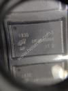
Part Number | STM8AL3LE88TCY |
---|---|
Manufacturer | STMicroelectronics |
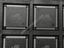
Description | IC MCU 8BIT 64KB FLASH 48LQFP |
Datasheet | STM8AL3LE88TCY Datasheet |
Package | 48-LQFP |
In Stock | 342 piece(s) |
Unit Price | $ 1.4784 * |
Lead Time | To be Confirmed |
Estimated Delivery Time | Jan 25 - Jan 30 (Choose Expedited Shipping) |
Request for Quotation |
|
Part Number # STM8AL3LE88TCY (Embedded - Microcontrollers) is manufactured by STMicroelectronics and distributed by Heisener. Being one of the leading electronics distributors, we carry many kinds of electronic components from some of the world’s top class manufacturers. Their quality is guaranteed by its stringent quality control to meet all required standards.
For STM8AL3LE88TCY specifications/configurations, quotation, lead time, payment terms of further enquiries please have no hesitation to contact us. To process your RFQ, please add STM8AL3LE88TCY with quantity into BOM. Heisener.com does NOT require any registration to request a quote of STM8AL3LE88TCY.
Manufacturer | STMicroelectronics |
Category | Integrated Circuits (ICs) - Embedded - Microcontrollers |
Datasheet | STM8AL3LE88TCYDatasheet |
Package | 48-LQFP |
Series | Automotive, AEC-Q100, STM8A |
Core Processor | STM8 |
Core Size | 8-Bit |
Speed | 16MHz |
Connectivity | I2C, IrDA, LIN, SPI, UART/USART |
Peripherals | Brown-out Detect/Reset, DMA, POR, PWM, WDT |
Number of I/O | 41 |
Program Memory Size | 64KB (64K x 8) |
Program Memory Type | FLASH |
EEPROM Size | 2K x 8 |
RAM Size | 4K x 8 |
Voltage - Supply (Vcc/Vdd) | 1.65 V ~ 3.6 V |
Data Converters | A/D 25x12b, D/A 2x12b |
Oscillator Type | Internal |
Operating Temperature | -40°C ~ 125°C (TA) |
Mounting Type | - |
Package / Case | 48-LQFP |
Supplier Device Package | 48-LQFP (7x7) |
This is information on a product in full production. December 2016 DocID027180 Rev 5 1/133 STM8AL31E8x STM8AL3LE8x Automotive 8-bit ultra-low-power MCU, 64 KB Flash, EEPROM, RTC, AES, LCD, timers, USARTs, I2C, SPIs, ADC, DAC, COMPs Datasheet - production data Features • AEC-Q100 grade 1 qualified • Operating conditions – Operating power supply range 1.8 V to 3.6 V (down to 1.65 V at power down) – Temp. range: -40 to 85 or 125 °C • Low-power features – 5 low-power modes: Wait, Low-power run (5.9 µA), Low-power wait (3 µA), Active- halt with full RTC (1.4 µA), Halt (400 nA) – Consumption: 200 µA/MHz+330 µA – Fast wake up from Halt mode (4.7 µs) – Ultra-low leakage per I/0: 50 nA • Advanced STM8 core – Harvard architecture and 3-stage pipeline – Max freq: 16 MHz, 16 CISC MIPS peak – Up to 40 external interrupt sources • Reset and supply management – Low power, ultra safe BOR reset with 5 programmable thresholds – Ultra-low-power POR/PDR – Programmable voltage detector (PVD) • Clock management – 32 kHz and 1-16 MHz crystal oscillators – Internal 16 MHz factory-trimmed RC and 38 kHz low consumption RC – Clock security system • Low-power RTC – BCD calendar with alarm interrupt, – Digital calibration with +/- 0.5ppm accuracy – Advanced anti-tamper detection • DMA – 4 ch. for ADC, encryption hardware accelerator (AES), DACs, SPIs, I2C, USARTs, Timers, 1 ch. for memory-to- memory • LCD: 8x40 or 4x44 w/ step-up converter • 12-bit ADC up to 1 Msps / 28 channels, – Temp. sensor and internal ref. voltage • Memories – Up to 64 Kbytes of Flash with up to 2 Kbytes of data EEPROM with ECC and RWW – Flexible write/read protection modes – Up to 4 Kbytes of RAM • 2x12-bit DAC (dual mode) with output buffer • 2 ultra-low-power comparators – 1 with fixed threshold and 1 rail to rail – Wakeup capability • Timers – Three 16-bit timers with 2 channels (IC, OC, PWM), quadrature encoder – One 16-bit advanced control timer with 3 channels, supporting motor control – One 8-bit timer with 7-bit prescaler – One window and one independent watchdog – Beeper timer with 1, 2 or 4 kHz frequencies • Communication interfaces – Two synchronous serial interface (SPI) – Fast I2C 400 kHz SMBus and PMBus – Three USARTs (IrDA, LIN 1.3, LIN2.0) • Up to 67 I/Os, all mappable on interrupt vectors • Fast on-chip programming and non-intrusive debugging with SWIM, Bootloader using USART • 96-bit unique ID LQFP80 LQFP64 LQFP48 14x14 mm 10x10 mm 7x7 mm www.st.com
STM8AL31E8x STM8AL3LE8x 2/133 DocID027180 Rev 5 Table 1. Device summary Reference Part number STM8AL31E8x STM8AL31E88, STM8AL31E89, STM8AL31E8A STM8AL3LE8x STM8AL3LE88, STM8AL3LE89, STM8AL3LE8A
DocID027180 Rev 5 3/133 STM8AL31E8x STM8AL3LE8x Contents 5 Contents 1 Introduction . . . . . . . . . . . . . . . . . . . . . . . . . . . . . . . . . . . . . . . . . . . . . . . 10 2 Description . . . . . . . . . . . . . . . . . . . . . . . . . . . . . . . . . . . . . . . . . . . . . . . . 11 2.1 STM8AL ultra-low-power 8-bit family benefits . . . . . . . . . . . . . . . . . . . . . .11 2.2 Device overview . . . . . . . . . . . . . . . . . . . . . . . . . . . . . . . . . . . . . . . . . . . . 13 3 Functional overview . . . . . . . . . . . . . . . . . . . . . . . . . . . . . . . . . . . . . . . . 14 3.1 Low-power modes . . . . . . . . . . . . . . . . . . . . . . . . . . . . . . . . . . . . . . . . . . 15 3.2 Central processing unit STM8 . . . . . . . . . . . . . . . . . . . . . . . . . . . . . . . . . 16 3.2.1 Advanced STM8 Core . . . . . . . . . . . . . . . . . . . . . . . . . . . . . . . . . . . . . . 16 3.2.2 Interrupt controller . . . . . . . . . . . . . . . . . . . . . . . . . . . . . . . . . . . . . . . . . 16 3.3 Reset and supply management . . . . . . . . . . . . . . . . . . . . . . . . . . . . . . . . 17 3.3.1 Power supply scheme . . . . . . . . . . . . . . . . . . . . . . . . . . . . . . . . . . . . . . 17 3.3.2 Power supply supervisor . . . . . . . . . . . . . . . . . . . . . . . . . . . . . . . . . . . . 17 3.3.3 Voltage regulator . . . . . . . . . . . . . . . . . . . . . . . . . . . . . . . . . . . . . . . . . . 18 3.4 Clock management . . . . . . . . . . . . . . . . . . . . . . . . . . . . . . . . . . . . . . . . . 18 3.5 Low-power real-time clock . . . . . . . . . . . . . . . . . . . . . . . . . . . . . . . . . . . . 19 3.6 LCD (Liquid crystal display) . . . . . . . . . . . . . . . . . . . . . . . . . . . . . . . . . . . 20 3.7 Memories . . . . . . . . . . . . . . . . . . . . . . . . . . . . . . . . . . . . . . . . . . . . . . . . . 20 3.8 DMA . . . . . . . . . . . . . . . . . . . . . . . . . . . . . . . . . . . . . . . . . . . . . . . . . . . . . 20 3.9 Analog-to-digital converter . . . . . . . . . . . . . . . . . . . . . . . . . . . . . . . . . . . . 21 3.10 Digital-to-analog converter . . . . . . . . . . . . . . . . . . . . . . . . . . . . . . . . . . . . 21 3.11 Ultra-low-power comparators . . . . . . . . . . . . . . . . . . . . . . . . . . . . . . . . . . 21 3.12 System configuration controller and routing interface . . . . . . . . . . . . . . . 22 3.13 AES . . . . . . . . . . . . . . . . . . . . . . . . . . . . . . . . . . . . . . . . . . . . . . . . . . . . . 22 3.14 Timers . . . . . . . . . . . . . . . . . . . . . . . . . . . . . . . . . . . . . . . . . . . . . . . . . . . 22 3.14.1 16-bit advanced control timer (TIM1) . . . . . . . . . . . . . . . . . . . . . . . . . . . 23 3.14.2 16-bit general purpose timers (TIM2, TIM3, TIM5) . . . . . . . . . . . . . . . . 23 3.14.3 8-bit basic timer (TIM4) . . . . . . . . . . . . . . . . . . . . . . . . . . . . . . . . . . . . . 23 3.15 Watchdog timers . . . . . . . . . . . . . . . . . . . . . . . . . . . . . . . . . . . . . . . . . . . 23 3.15.1 Window watchdog timer . . . . . . . . . . . . . . . . . . . . . . . . . . . . . . . . . . . . . 23 3.15.2 Independent watchdog timer . . . . . . . . . . . . . . . . . . . . . . . . . . . . . . . . . 23
Contents STM8AL31E8x STM8AL3LE8x 4/133 DocID027180 Rev 5 3.16 Beeper . . . . . . . . . . . . . . . . . . . . . . . . . . . . . . . . . . . . . . . . . . . . . . . . . . . 24 3.17 Communication interfaces . . . . . . . . . . . . . . . . . . . . . . . . . . . . . . . . . . . . 24 3.17.1 SPI . . . . . . . . . . . . . . . . . . . . . . . . . . . . . . . . . . . . . . . . . . . . . . . . . . . . . 24 3.17.2 I2C . . . . . . . . . . . . . . . . . . . . . . . . . . . . . . . . . . . . . . . . . . . . . . . . . . . . . 24 3.17.3 USART . . . . . . . . . . . . . . . . . . . . . . . . . . . . . . . . . . . . . . . . . . . . . . . . . . 25 3.18 Infrared (IR) interface . . . . . . . . . . . . . . . . . . . . . . . . . . . . . . . . . . . . . . . . 25 3.19 Development support . . . . . . . . . . . . . . . . . . . . . . . . . . . . . . . . . . . . . . . . 25 4 Pin description . . . . . . . . . . . . . . . . . . . . . . . . . . . . . . . . . . . . . . . . . . . . 27 5 Memory and register map . . . . . . . . . . . . . . . . . . . . . . . . . . . . . . . . . . . . 39 5.1 Memory mapping . . . . . . . . . . . . . . . . . . . . . . . . . . . . . . . . . . . . . . . . . . . 39 5.2 Register map . . . . . . . . . . . . . . . . . . . . . . . . . . . . . . . . . . . . . . . . . . . . . . 40 6 Interrupt vector mapping . . . . . . . . . . . . . . . . . . . . . . . . . . . . . . . . . . . . 60 7 Option byte . . . . . . . . . . . . . . . . . . . . . . . . . . . . . . . . . . . . . . . . . . . . . . . 62 8 Unique ID . . . . . . . . . . . . . . . . . . . . . . . . . . . . . . . . . . . . . . . . . . . . . . . . . 65 9 Electrical parameters . . . . . . . . . . . . . . . . . . . . . . . . . . . . . . . . . . . . . . . 66 9.1 Parameter conditions . . . . . . . . . . . . . . . . . . . . . . . . . . . . . . . . . . . . . . . . 66 9.1.1 Minimum and maximum values . . . . . . . . . . . . . . . . . . . . . . . . . . . . . . . 66 9.1.2 Typical values . . . . . . . . . . . . . . . . . . . . . . . . . . . . . . . . . . . . . . . . . . . . 66 9.1.3 Typical curves . . . . . . . . . . . . . . . . . . . . . . . . . . . . . . . . . . . . . . . . . . . . 66 9.1.4 Loading capacitor . . . . . . . . . . . . . . . . . . . . . . . . . . . . . . . . . . . . . . . . . 66 9.1.5 Pin input voltage . . . . . . . . . . . . . . . . . . . . . . . . . . . . . . . . . . . . . . . . . . 67 9.2 Absolute maximum ratings . . . . . . . . . . . . . . . . . . . . . . . . . . . . . . . . . . . . 67 9.3 Operating conditions . . . . . . . . . . . . . . . . . . . . . . . . . . . . . . . . . . . . . . . . 69 9.3.1 General operating conditions . . . . . . . . . . . . . . . . . . . . . . . . . . . . . . . . . 69 9.3.2 Embedded reset and power control block characteristics . . . . . . . . . . 70 9.3.3 Supply current characteristics . . . . . . . . . . . . . . . . . . . . . . . . . . . . . . . . 72 9.3.4 Clock and timing characteristics . . . . . . . . . . . . . . . . . . . . . . . . . . . . . . 85 9.3.5 Memory characteristics . . . . . . . . . . . . . . . . . . . . . . . . . . . . . . . . . . . . . 90 9.3.6 I/O current injection characteristics . . . . . . . . . . . . . . . . . . . . . . . . . . . . 92 9.3.7 I/O port pin characteristics . . . . . . . . . . . . . . . . . . . . . . . . . . . . . . . . . . . 92 9.3.8 Communication interfaces . . . . . . . . . . . . . . . . . . . . . . . . . . . . . . . . . . 100
DocID027180 Rev 5 5/133 STM8AL31E8x STM8AL3LE8x Contents 5 9.3.9 LCD controller (STM8AL3LE8x only) . . . . . . . . . . . . . . . . . . . . . . . . . . 105 9.3.10 Embedded reference voltage . . . . . . . . . . . . . . . . . . . . . . . . . . . . . . . . 106 9.3.11 Temperature sensor . . . . . . . . . . . . . . . . . . . . . . . . . . . . . . . . . . . . . . . 107 9.3.12 Comparator characteristics . . . . . . . . . . . . . . . . . . . . . . . . . . . . . . . . . 107 9.3.13 12-bit DAC characteristics . . . . . . . . . . . . . . . . . . . . . . . . . . . . . . . . . . 109 9.3.14 12-bit ADC1 characteristics . . . . . . . . . . . . . . . . . . . . . . . . . . . . . . . . . 112 9.3.15 EMC characteristics . . . . . . . . . . . . . . . . . . . . . . . . . . . . . . . . . . . . . . . 117 9.4 Thermal characteristics . . . . . . . . . . . . . . . . . . . . . . . . . . . . . . . . . . . . . .119 10 Package information . . . . . . . . . . . . . . . . . . . . . . . . . . . . . . . . . . . . . . . 120 10.1 LQFP80 package information . . . . . . . . . . . . . . . . . . . . . . . . . . . . . . . . . 120 10.2 LQFP64 package information . . . . . . . . . . . . . . . . . . . . . . . . . . . . . . . . . 124 10.3 LQFP48 package information . . . . . . . . . . . . . . . . . . . . . . . . . . . . . . . . . 127 11 Ordering information . . . . . . . . . . . . . . . . . . . . . . . . . . . . . . . . . . . . . . 131 12 Revision history . . . . . . . . . . . . . . . . . . . . . . . . . . . . . . . . . . . . . . . . . . 132
List of tables STM8AL31E8x STM8AL3LE8x 6/133 DocID027180 Rev 5 List of tables Table 1. Device summary . . . . . . . . . . . . . . . . . . . . . . . . . . . . . . . . . . . . . . . . . . . . . . . . . . . . . . . . . . 2 Table 2. High-density STM8AL3xE8x low-power device features and peripheral counts. . . . . . . . . 13 Table 3. Timer feature comparison. . . . . . . . . . . . . . . . . . . . . . . . . . . . . . . . . . . . . . . . . . . . . . . . . . 22 Table 4. Legend/abbreviation . . . . . . . . . . . . . . . . . . . . . . . . . . . . . . . . . . . . . . . . . . . . . . . . . . . . . . 30 Table 5. High-density STM8AL3xE8x pin description. . . . . . . . . . . . . . . . . . . . . . . . . . . . . . . . . . . . 30 Table 6. Flash and RAM boundary addresses . . . . . . . . . . . . . . . . . . . . . . . . . . . . . . . . . . . . . . . . . 40 Table 7. Factory conversion registers. . . . . . . . . . . . . . . . . . . . . . . . . . . . . . . . . . . . . . . . . . . . . . . . 40 Table 8. I/O port hardware register map. . . . . . . . . . . . . . . . . . . . . . . . . . . . . . . . . . . . . . . . . . . . . . 40 Table 9. General hardware register map . . . . . . . . . . . . . . . . . . . . . . . . . . . . . . . . . . . . . . . . . . . . . 42 Table 10. CPU/SWIM/debug module/interrupt controller registers . . . . . . . . . . . . . . . . . . . . . . . . . . . 58 Table 11. Interrupt mapping . . . . . . . . . . . . . . . . . . . . . . . . . . . . . . . . . . . . . . . . . . . . . . . . . . . . . . . . 60 Table 12. Option byte addresses . . . . . . . . . . . . . . . . . . . . . . . . . . . . . . . . . . . . . . . . . . . . . . . . . . . . 62 Table 13. Option byte description . . . . . . . . . . . . . . . . . . . . . . . . . . . . . . . . . . . . . . . . . . . . . . . . . . . . 63 Table 14. Unique ID registers (96 bits) . . . . . . . . . . . . . . . . . . . . . . . . . . . . . . . . . . . . . . . . . . . . . . . . 65 Table 15. Voltage characteristics . . . . . . . . . . . . . . . . . . . . . . . . . . . . . . . . . . . . . . . . . . . . . . . . . . . . 67 Table 16. Current characteristics . . . . . . . . . . . . . . . . . . . . . . . . . . . . . . . . . . . . . . . . . . . . . . . . . . . . 68 Table 17. Thermal characteristics. . . . . . . . . . . . . . . . . . . . . . . . . . . . . . . . . . . . . . . . . . . . . . . . . . . . 68 Table 18. Operating lifetime (OLF) . . . . . . . . . . . . . . . . . . . . . . . . . . . . . . . . . . . . . . . . . . . . . . . . . . . 68 Table 19. General operating conditions . . . . . . . . . . . . . . . . . . . . . . . . . . . . . . . . . . . . . . . . . . . . . . . 69 Table 20. Embedded reset and power control block characteristics. . . . . . . . . . . . . . . . . . . . . . . . . . 70 Table 21. Total current consumption in Run mode. . . . . . . . . . . . . . . . . . . . . . . . . . . . . . . . . . . . . . . 72 Table 22. Total current consumption in Wait mode . . . . . . . . . . . . . . . . . . . . . . . . . . . . . . . . . . . . . . 75 Table 23. Total current consumption and timing in low-power run mode at VDD = 1.65 V to 3.6 V . . . . . . . . . . . . . . . . . . . . . . . . . . . . . . . . . . . . . . . . . . . . . . . . . . . . . . . . . . . . . . . 77 Table 24. Total current consumption in low-power wait mode at VDD = 1.65 V to 3.6 V . . . . . . . . . . 78 Table 25. Total current consumption and timing in Active-halt mode at VDD = 1.65 V to 3.6 V . . . . . . . . . . . . . . . . . . . . . . . . . . . . . . . . . . . . . . . . . . . . . . . . . . 79 Table 26. Typical current consumption in Active-halt mode, RTC clocked by LSE external crystal . . 80 Table 27. Total current consumption and timing in Halt mode at VDD = 1.65 to 3.6 V . . . . . . . . . . . 82 Table 28. Peripheral current consumption . . . . . . . . . . . . . . . . . . . . . . . . . . . . . . . . . . . . . . . . . . . . . 83 Table 29. Current consumption under external reset . . . . . . . . . . . . . . . . . . . . . . . . . . . . . . . . . . . . . 85 Table 30. HSE external clock characteristics . . . . . . . . . . . . . . . . . . . . . . . . . . . . . . . . . . . . . . . . . . . 85 Table 31. LSE external clock characteristics . . . . . . . . . . . . . . . . . . . . . . . . . . . . . . . . . . . . . . . . . . . 86 Table 32. HSE oscillator characteristics . . . . . . . . . . . . . . . . . . . . . . . . . . . . . . . . . . . . . . . . . . . . . . . 86 Table 33. LSE oscillator characteristics . . . . . . . . . . . . . . . . . . . . . . . . . . . . . . . . . . . . . . . . . . . . . . . 88 Table 34. HSI oscillator characteristics. . . . . . . . . . . . . . . . . . . . . . . . . . . . . . . . . . . . . . . . . . . . . . . . 89 Table 35. LSI oscillator characteristics . . . . . . . . . . . . . . . . . . . . . . . . . . . . . . . . . . . . . . . . . . . . . . . . 90 Table 36. RAM and hardware registers . . . . . . . . . . . . . . . . . . . . . . . . . . . . . . . . . . . . . . . . . . . . . . . 90 Table 37. Flash program memory/data EEPROM memory . . . . . . . . . . . . . . . . . . . . . . . . . . . . . . . . 91 Table 38. Flash program memory. . . . . . . . . . . . . . . . . . . . . . . . . . . . . . . . . . . . . . . . . . . . . . . . . . . . 91 Table 39. Data memory . . . . . . . . . . . . . . . . . . . . . . . . . . . . . . . . . . . . . . . . . . . . . . . . . . . . . . . . . . . 91 Table 40. I/O current injection susceptibility . . . . . . . . . . . . . . . . . . . . . . . . . . . . . . . . . . . . . . . . . . . . 92 Table 41. I/O static characteristics . . . . . . . . . . . . . . . . . . . . . . . . . . . . . . . . . . . . . . . . . . . . . . . . . . . 93 Table 42. Output driving current (high sink ports). . . . . . . . . . . . . . . . . . . . . . . . . . . . . . . . . . . . . . . . 96 Table 43. Output driving current (true open drain ports). . . . . . . . . . . . . . . . . . . . . . . . . . . . . . . . . . . 96 Table 44. Output driving current (PA0 with high sink LED driver capability). . . . . . . . . . . . . . . . . . . . 96 Table 45. NRST pin characteristics . . . . . . . . . . . . . . . . . . . . . . . . . . . . . . . . . . . . . . . . . . . . . . . . . . 98 Table 46. SPI1 characteristics . . . . . . . . . . . . . . . . . . . . . . . . . . . . . . . . . . . . . . . . . . . . . . . . . . . . . 100
DocID027180 Rev 5 7/133 STM8AL31E8x STM8AL3LE8x List of tables 7 Table 47. I2C characteristics . . . . . . . . . . . . . . . . . . . . . . . . . . . . . . . . . . . . . . . . . . . . . . . . . . . . . . 103 Table 48. LCD characteristics. . . . . . . . . . . . . . . . . . . . . . . . . . . . . . . . . . . . . . . . . . . . . . . . . . . . . . 105 Table 49. Reference voltage characteristics. . . . . . . . . . . . . . . . . . . . . . . . . . . . . . . . . . . . . . . . . . . 106 Table 50. TS characteristics . . . . . . . . . . . . . . . . . . . . . . . . . . . . . . . . . . . . . . . . . . . . . . . . . . . . . . . 107 Table 51. Comparator 1 characteristics . . . . . . . . . . . . . . . . . . . . . . . . . . . . . . . . . . . . . . . . . . . . . . 107 Table 52. Comparator 2 characteristics . . . . . . . . . . . . . . . . . . . . . . . . . . . . . . . . . . . . . . . . . . . . . . 108 Table 53. DAC characteristics . . . . . . . . . . . . . . . . . . . . . . . . . . . . . . . . . . . . . . . . . . . . . . . . . . . . . 109 Table 54. DAC accuracy. . . . . . . . . . . . . . . . . . . . . . . . . . . . . . . . . . . . . . . . . . . . . . . . . . . . . . . . . . 110 Table 55. DAC output on PB4-PB5-PB6 . . . . . . . . . . . . . . . . . . . . . . . . . . . . . . . . . . . . . . . . . . . . . 111 Table 56. ADC1 characteristics . . . . . . . . . . . . . . . . . . . . . . . . . . . . . . . . . . . . . . . . . . . . . . . . . . . . 112 Table 57. ADC1 accuracy with VDDA = 3.3 V to 2.5 V. . . . . . . . . . . . . . . . . . . . . . . . . . . . . . . . . . . 114 Table 58. ADC1 accuracy with VDDA = 2.4 V to 3.6 V. . . . . . . . . . . . . . . . . . . . . . . . . . . . . . . . . . . 114 Table 59. ADC1 accuracy with VDDA = VREF+ = 1.8 V to 2.4 V. . . . . . . . . . . . . . . . . . . . . . . . . . . 114 Table 60. EMS data . . . . . . . . . . . . . . . . . . . . . . . . . . . . . . . . . . . . . . . . . . . . . . . . . . . . . . . . . . . . . 117 Table 61. EMI data . . . . . . . . . . . . . . . . . . . . . . . . . . . . . . . . . . . . . . . . . . . . . . . . . . . . . . . . . . . . . 118 Table 62. ESD absolute maximum ratings . . . . . . . . . . . . . . . . . . . . . . . . . . . . . . . . . . . . . . . . . . . . 118 Table 63. Electrical sensitivities . . . . . . . . . . . . . . . . . . . . . . . . . . . . . . . . . . . . . . . . . . . . . . . . . . . . 119 Table 64. Thermal characteristics. . . . . . . . . . . . . . . . . . . . . . . . . . . . . . . . . . . . . . . . . . . . . . . . . . . 119 Table 65. LQFP80 - 80-pin, 14 x 14 mm low-profile quad flat package mechanical data . . . . . . . . . . . . . . . . . . . . . . . . . . . . . . . . . . . . . . . . . . . . . . . . . . . . . . . . 121 Table 66. LQFP64 - 64-pin, 10 x 10 mm low-profile quad flat package mechanical data . . . . . . . . . . . . . . . . . . . . . . . . . . . . . . . . . . . . . . . . . . . . . . . . . 124 Table 67. LQFP48 - 48-pin, 7 x 7 mm low-profile quad flat package mechanical data . . . . . . . . . . . . . . . . . . . . . . . . . . . . . . . . . . . . . . . . . . . . . . . . . . . . . . . . 128 Table 68. STM8AL31E8x STM8AL3LE8x ordering information scheme . . . . . . . . . . . . . . . . . . . . . 131 Table 69. Document revision history . . . . . . . . . . . . . . . . . . . . . . . . . . . . . . . . . . . . . . . . . . . . . . . . 132
List of figures STM8AL31E8x STM8AL3LE8x 8/133 DocID027180 Rev 5 List of figures Figure 1. High-density STM8AL3xE8x device block diagram . . . . . . . . . . . . . . . . . . . . . . . . . . . . . . 14 Figure 2. Clock tree diagram . . . . . . . . . . . . . . . . . . . . . . . . . . . . . . . . . . . . . . . . . . . . . . . . . . . . . . . 19 Figure 3. STM8AL31E8A 80-pin package pinout (without LCD) . . . . . . . . . . . . . . . . . . . . . . . . . . . . 27 Figure 4. STM8AL3LE8A 80-pin package pinout (with LCD). . . . . . . . . . . . . . . . . . . . . . . . . . . . . . . 27 Figure 5. STM8AL31E89 64-pin pinout (without LCD). . . . . . . . . . . . . . . . . . . . . . . . . . . . . . . . . . . . 28 Figure 6. STM8AL3LE89 64-pin pinout (with LCD) . . . . . . . . . . . . . . . . . . . . . . . . . . . . . . . . . . . . . . 28 Figure 7. STM8AL31E88 48-pin pinout (without LCD) . . . . . . . . . . . . . . . . . . . . . . . . . . . . . . . . . . . 29 Figure 8. STM8AL3LE88 48-pin pinout (with LCD) . . . . . . . . . . . . . . . . . . . . . . . . . . . . . . . . . . . . . . 29 Figure 9. Memory map . . . . . . . . . . . . . . . . . . . . . . . . . . . . . . . . . . . . . . . . . . . . . . . . . . . . . . . . . . . 39 Figure 10. Pin loading conditions. . . . . . . . . . . . . . . . . . . . . . . . . . . . . . . . . . . . . . . . . . . . . . . . . . . . . 66 Figure 11. Pin input voltage . . . . . . . . . . . . . . . . . . . . . . . . . . . . . . . . . . . . . . . . . . . . . . . . . . . . . . . . . 67 Figure 12. Power supply thresholds. . . . . . . . . . . . . . . . . . . . . . . . . . . . . . . . . . . . . . . . . . . . . . . . . . . 71 Figure 13. Typical IDD(RUN) from RAM vs. VDD (HSI clock source), fCPU =16 MHz (1) . . . . . . . . . . . . . 73 Figure 14. Typical IDD(RUN) from Flash vs. VDD (HSI clock source), fCPU = 16 MHz (1) . . . . . . . . . . . . 74 Figure 15. Typical IDD(Wait) from RAM vs. VDD (HSI clock source), fCPU = 16 MHz (1) . . . . . . . . . . . . . 76 Figure 16. Typical IDD(Wait) from Flash (HSI clock source), fCPU = 16 MHz (1) . . . . . . . . . . . . . . . . . . . 76 Figure 17. Typical IDD(LPR) vs. VDD (LSI clock source), all peripherals OFF . . . . . . . . . . . . . . . . . . . . 77 Figure 18. Typical IDD(LPW) vs. VDD (LSI clock source), all peripherals OFF (1) . . . . . . . . . . . . . . . . . . 78 Figure 19. Typical IDD(AH) vs. VDD (LSI clock source) . . . . . . . . . . . . . . . . . . . . . . . . . . . . . . . . . . . 81 Figure 20. Typical IDD(Halt) vs. VDD (internal reference voltage OFF) . . . . . . . . . . . . . . . . . . . . . . . . 82 Figure 21. HSE oscillator circuit diagram. . . . . . . . . . . . . . . . . . . . . . . . . . . . . . . . . . . . . . . . . . . . . . . 87 Figure 22. LSE oscillator circuit diagram . . . . . . . . . . . . . . . . . . . . . . . . . . . . . . . . . . . . . . . . . . . . . . . 88 Figure 23. Typical HSI frequency vs. VDD . . . . . . . . . . . . . . . . . . . . . . . . . . . . . . . . . . . . . . . . . . . . . . 89 Figure 24. Typical LSI clock source frequency vs. VDD . . . . . . . . . . . . . . . . . . . . . . . . . . . . . . . . . . . 90 Figure 25. Typical VIL and VIH vs. VDD (standard I/Os) . . . . . . . . . . . . . . . . . . . . . . . . . . . . . . . . . . . 94 Figure 26. Typical VIL and VIH vs. VDD (true open drain I/Os). . . . . . . . . . . . . . . . . . . . . . . . . . . . . . 94 Figure 27. Typical pull-up resistance RPU vs. VDD with VIN=VSS. . . . . . . . . . . . . . . . . . . . . . . . . . . . 95 Figure 28. Typical pull-up current Ipu vs. VDD with VIN=VSS . . . . . . . . . . . . . . . . . . . . . . . . . . . . . . . 95 Figure 29. Typical VOL @ VDD = 3.0 V (high sink ports) . . . . . . . . . . . . . . . . . . . . . . . . . . . . . . . . . . 97 Figure 30. Typical VOL @ VDD = 1.8 V (high sink ports) . . . . . . . . . . . . . . . . . . . . . . . . . . . . . . . . . . 97 Figure 31. Typical VOL @ VDD = 3.0 V (true open drain ports) . . . . . . . . . . . . . . . . . . . . . . . . . . . . . 97 Figure 32. Typical VOL @ VDD = 1.8 V (true open drain ports) . . . . . . . . . . . . . . . . . . . . . . . . . . . . . 97 Figure 33. Typical VDD - VOH @ VDD = 3.0 V (high sink ports). . . . . . . . . . . . . . . . . . . . . . . . . . . . . 97 Figure 34. Typical VDD - VOH @ VDD = 1.8 V (high sink ports). . . . . . . . . . . . . . . . . . . . . . . . . . . . . 97 Figure 35. Typical NRST pull-up resistance RPU vs. VDD . . . . . . . . . . . . . . . . . . . . . . . . . . . . . . . . . . 98 Figure 36. Typical NRST pull-up current Ipu vs. VDD . . . . . . . . . . . . . . . . . . . . . . . . . . . . . . . . . . . . . 99 Figure 37. Recommended NRST pin configuration . . . . . . . . . . . . . . . . . . . . . . . . . . . . . . . . . . . . . . . 99 Figure 38. SPI1 timing diagram - slave mode and CPHA=0 . . . . . . . . . . . . . . . . . . . . . . . . . . . . . . . 101 Figure 39. SPI1 timing diagram - slave mode and CPHA=1(1) . . . . . . . . . . . . . . . . . . . . . . . . . . . . . 101 Figure 40. SPI1 timing diagram - master mode(1) . . . . . . . . . . . . . . . . . . . . . . . . . . . . . . . . . . . . . . . 102 Figure 41. Typical application with I2C bus and timing diagram(1)) . . . . . . . . . . . . . . . . . . . . . . . . . . 104 Figure 42. ADC1 accuracy characteristics . . . . . . . . . . . . . . . . . . . . . . . . . . . . . . . . . . . . . . . . . . . . . 115 Figure 43. Typical connection diagram using the ADC . . . . . . . . . . . . . . . . . . . . . . . . . . . . . . . . . . . 115 Figure 44. Power supply and reference decoupling (VREF+ not connected to VDDA). . . . . . . . . . . . . 116 Figure 45. Power supply and reference decoupling (VREF+ connected to VDDA) . . . . . . . . . . . . . . 116 Figure 46. LQFP80 - 80-pin, 14 x 14 mm low-profile quad flat package outline . . . . . . . . . . . . . . . . 120 Figure 47. LQFP80 - 80-pin, 14 x 14 mm low-profile quad flat package recommended footprint . . . . . . . . . . . . . . . . . . . . . . . . . . . . . . . . . . . . . . . . . . . . . . . . . . . 122
DocID027180 Rev 5 9/133 STM8AL31E8x STM8AL3LE8x List of figures 9 Figure 48. LQFP80 marking example (package top view) . . . . . . . . . . . . . . . . . . . . . . . . . . . . . . . . . 123 Figure 49. LQFP64 - 64-pin, 10 x 10 mm low-profile quad flat package outline . . . . . . . . . . . . . . . . 124 Figure 50. LQFP64 - 64-pin, 10 x 10 mm low-profile quad flat package recommended footprint . . . . . . . . . . . . . . . . . . . . . . . . . . . . . . . . . . . . . . . . . . . . . . . . . . . 125 Figure 51. LQFP64 marking example (package top view) . . . . . . . . . . . . . . . . . . . . . . . . . . . . . . . . . 126 Figure 52. LQFP48 - 48-pin, 7 x 7 mm low-profile quad flat package outline . . . . . . . . . . . . . . . . . . 127 Figure 53. LQFP48 - 48-pin, 7 x 7 mm low-profile quad flat package recommended footprint . . . . . . . . . . . . . . . . . . . . . . . . . . . . . . . . . . . . . . . . . . . . . . . . . . . 129 Figure 54. LQFP48 marking example (package top view) . . . . . . . . . . . . . . . . . . . . . . . . . . . . . . . . . 130
Grace*****Sandhu
December 21, 2020
Alm*****aller
December 20, 2020
Zai*****aran
December 17, 2020
Jenn***** Xiong
December 9, 2020
Damo*****ashad
November 19, 2020
Rey*****Berry
November 14, 2020
Luk*****Lam
November 10, 2020
Brayd*****tersen
November 9, 2020
We guarantee 100% customer satisfaction.
Our experienced sales team and tech support team back our services to satisfy all our customers.
We provide 90 days warranty.
If the items you received were not in perfect quality, we would be responsible for your refund or replacement, but the items must be returned in their original condition.
Payment Methods | |
Delivery Services |
Heisener's commitment to quality has shaped our processes for sourcing, testing, shipping, and every step in between. This foundation underlies each component we sell.