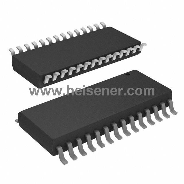
Product description
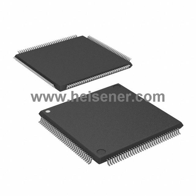
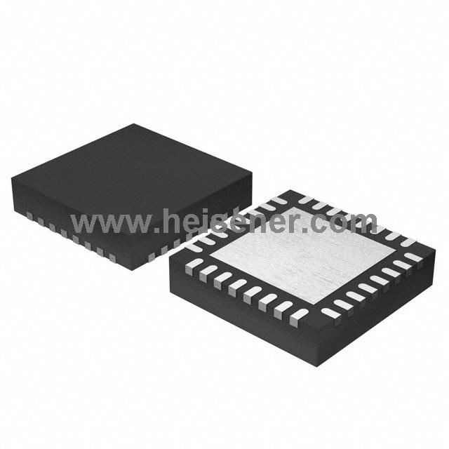
The AD6645 is a high-speed, high-performance, monolithic 14-bit analog-to-digital converter (ADC). Analog Devices ultra-fast complementary bipolar (XFCB) process with an innovative multiplex architecture. Units are available in 52 Lead Exposure Pads (TQFP_EP) packaging with specified ranges −40°C to +85°C, at 80 MSPS and −10°C to +85°C, at 105 MSPS.
The chip contains all the necessary features, including Trace and Hold (T/H) and reference, to provide a complete conversion solution. The AD6645 offers cmos compatible digital output. It is the fourth generation of the broadband ADC family, preceded by AD9042(12-bit, 41 MSPS), AD6640(12-bit, 65 MSPS, IF sampling), and AD6644(14-bit, 40 MSPS/65 MSPS).
The AD6645 is part of the Analog Devices SoftCell transceiver chipset designed for multi-channel, multi-mode receivers. The AD6645 maintains a 100 dB multitone spury-free dynamic range (SFDR) over the second Nyquist band. This breakthrough performance relieves the burden on multimodule digital word receivers (software radios) that are usually limited by ADCs. Excellent noise performance; The typical signal-to-noise ratio (SNR) across the first Nyquist band is 74.5 dB.
AD6645 Pin arrangement

Working principle
The AD6645 ADC employs a three-stage subrange architecture. This design approach achieves the required accuracy and speed while maintaining low power and small die size. As shown in the functional block diagram (see functional block diagram)
The AD6645 has complementary analog input pins, AIN and AIN. Each analog input is centered at 2.4V and should swing ± 0.55V around this reference (see the picture below).
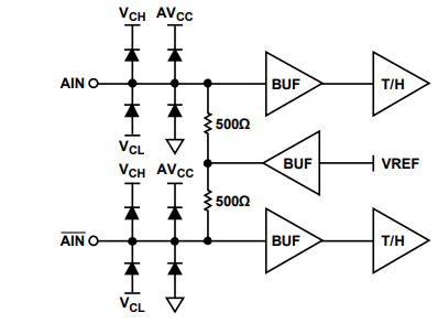
Because AIN and AIN are 180° out of phase, Because ain and ain are 180° out of phase, the differential analog input signal is 2.2 V p-p. Both analog inputs are buffered prior to the first track-and-hold, The differential analog input signal is 2.2 v p-p. Both analog inputs are buffered prior to the first track-and-hold, TH1. The high state of the encode pulse places TH1 in hold mode. The held value of TH1 is applied to the input of a 5-bit coarse ADC1.
The digital output of ADC1 drives a 5-bit digitalto-analog converter, DAC1. DAC1 requires 14 bits of precision that is achieved through laser trimming. The output of DAC1 is subtracted from the delayed analog signal at the input of TH3 to generate a first residue signal. TH2 provides an analog pipeline delay to compensate for the digital delay of ADC1.
The first residual signal is applied to a second conversion stage consisting of a 5-bit ADC2, a 5-bit DAC2, and a pipeline TH4. The second DAC requires 10 bits of precision, which is met by the process with no trim. The input to TH5 is a second residual signal generated by subtracting the quantized output of DAC2 from the first residual signal held by TH4. TH5 drives a final 6-bit ADC3.
The digital outputs from ADC1, ADC2, and ADC3 are added together and corrected in the digital error correction logic to generate the final output data. The result is a 14-bit parallel digital CMOS-compatible word, coded as twos complement
AD6645 Functional block diagram

Product characteristics
(1) If sampling. The AD6645 maintains excellent AC performance at an input frequency of 200 MHz and is suitable for multi-carrier 3G broadband cellular IF sampling receivers.
(2) Marketing compatibility. The ADC features the same footprint and pin layout as the AD6644 14-bit, 40 MSPS/65 MSPS ADC.
(3) SFDR performance and oversampling. The multitone SFDR performance of 100 dBFS reduces the need for high-end RF components.
AD6645 Applications
● Multi-channel, multi-mode receiver
● Base station infrastructure
● Ampere, is-136, cdma, gsm, w-cdma
● Single channel digital receiver
● Array processing
● Communication instrument
● Radar, infrared imaging
● Instrument