A memory controller is a hardware component responsible for managing communication with memory. It is located in the CPU or the northbridge chip, and in modern systems, it is usually integrated directly into the CPU. The memory controller handles tasks such as receiving read and write requests from the CPU, translating these requests into commands that the memory modules can understand, managing memory addressing, controlling memory refresh cycles, and handling data transfers.
Memory Controller Operating Principle
The memory controller is a critical component within a computer system that manages memory operations and handles data exchange between the memory and the CPU. It determines key parameters such as the maximum supported memory capacity, number of memory banks, memory type and speed, memory chip data depth, and data width. In other words, the memory controller defines the system’s memory performance and therefore has a significant impact on overall system performance.
1. Working Principle of the Memory Controller
The memory controller is integrated into the CPU, allowing it to operate at the same frequency as the CPU cores. With this design, data transfers between the CPU and memory no longer need to pass through the northbridge, which effectively reduces latency and greatly improves data processing efficiency and overall system performance. This is similar to placing a warehouse directly next to a production workshop to boost efficiency.
2. Key Performance Parameters
Frequency and Capacity:
The memory clock speed (such as 1600 MHz for DDR3 or 2133 MHz for DDR4) determines the maximum stable operating speed. Memory capacity (for example, 8 GB or 16 GB per module) directly affects system responsiveness and multitasking capability.
Operating Voltage:
Different memory types have specific voltage requirements (for example, DDR3 typically operates at around 1.5 V or 1.35 V). Slightly increasing the voltage can help with overclocking, but it also increases heat generation and the risk of hardware damage.
3. Memory Timing Parameters (Example: 8-8-8-24)
Memory timings are determined by the delay cycles involved in row and column addressing. Smaller values generally indicate better performance:
- tCL (CAS Latency): The first parameter, representing the delay between a read/write command and actual data execution. It has the greatest impact on performance.
- tRCD (RAS to CAS Delay): The second parameter, indicating the delay between row addressing and column addressing.
- tRP (Row Precharge Time): The third parameter, referring to the time required to precharge a row before accessing another one. Lower values allow faster read/write operations.
- tRAS (Minimum RAS Active Time): The fourth parameter, defining the minimum time a row must remain active before precharging. Setting it too long reduces performance, while setting it too short may cause data loss.
Types of Memory Controllers
With the development of computer technology, memory controllers can be divided into two types: the traditional type and the integrated type.
Traditional Type
In traditional computer systems, the memory controller is located in the motherboard chipset’s northbridge. When the CPU exchanges data with memory, the data path follows five steps: CPU → Northbridge → Memory → Northbridge → CPU. Because the data must pass through multiple stages, the latency is relatively high, which negatively affects overall system performance.
Integrated Type
An Integrated Memory Controller (IMC) means that the memory controller is built directly into the CPU instead of being placed in the northbridge chip.
In systems without an integrated memory controller, the CPU accesses memory through the northbridge. The northbridge handles memory addressing and data access, then transfers the data to the CPU via the Front Side Bus (FSB). Although memory-to-northbridge access may be fast, the limited FSB bandwidth adds extra delay, creating a performance bottleneck.
When the memory controller is integrated into the CPU, memory data can be delivered directly to the controller inside the CPU without passing through the northbridge or the FSB. For the same 12GB of data, the transfer can be completed in about 1 second, greatly reducing latency, improving memory bandwidth utilization, and significantly enhancing overall CPU performance.

Structure of Memory Controllers(SDRAM)
The detailed functional block diagram of the memory controller is shown below:

As illustrated in the block diagram above, the front-end and back-end of the memory controller consist of four primary modules: Memory Map, Arbiter, Command Generator, and Data Path.
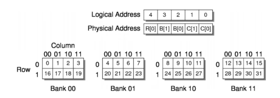
When a request is sent within the system, the Memory Map module initiates its process by converting the logical addresses used in the program into DDR physical addresses, specifying the exact bank, row, and column.

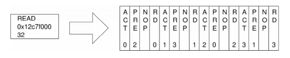
After the address translation is completed, the Arbiter determines which request to prioritize based on its priority level. Once the Arbiter has finalized the decision, the Command Generator converts the mapped memory request into commands that the DDR can execute, specifically the aforementioned activation, read/write, precharge, and refresh operations. Finally, the DDR performs the actual writing or reading of the required data, which is input and output through the Data Path via the data bus.
Memory Map
Memory map is the process of translating the CPU's logical addresses into DDR physical addresses. The physical addresses include row, column, and bank information, thereby completing a one-time mapping from logical addresses to specific locations in DDR.
Arbiter
An arbiter acts like a commander, queuing and scheduling requests when multiple commands access memory simultaneously. An efficient arbiter must balance efficiency, predictability, decision speed, fairness, and flexibility, but these traits are hard to achieve all at once. For example, complete fairness reduces efficiency.
Command Generator
System instructions are abstract requests. The command generator translates them into DDR-executable instruction sequences that follow the timing parameters specified in the memory datasheet. When the DDR chip is replaced, the same system instruction may result in different DDR actions due to differences in the instruction set.
Data Path
After DDR completes an operation, the data needs to be returned to the system via the data bus. An efficient memory controller keeps the data bus continuously busy to maximize performance.
Memory Controller Pros and Cons
With the development of CPU technology, integrating the memory controller into the CPU has become a trend. This design can improve system performance and reduce the load on the Northbridge, but it also introduces limitations in flexibility and compatibility.
Pros
1. An integrated memory controller allows the CPU and memory controller to run at the same frequency, enabling data exchange without passing through the Northbridge, which reduces latency and improves overall performance.
2. It reduces the workload on the Northbridge, allowing it to more efficiently support other data channels such as SATA and PCI-E.
Cons
The integrated memory controller has limited adaptability, supporting only specific types, capacities, and speeds of memory. Updating to a new memory type requires replacing the CPU. In contrast, traditional Northbridge-based controllers are more flexible, as simply replacing the motherboard can enable support for new memory.
 0
0







 Login/Register
 BOM
BOM
 Cart
Cart