IDT5V49EE902 is a programmable clock generator for high performance data communications, telecommunications, consumer and networking applications. There are four internal PLLS, each individually programmable to allow for four unique non-integer correlated frequencies. The frequency is generated by a single reference clock. The reference clock can come from one of two redundant clock inputs. Automatic or manual switching allows the selection of any redundant clock during normal operation.
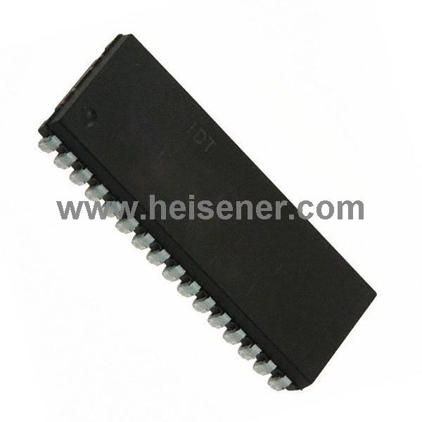
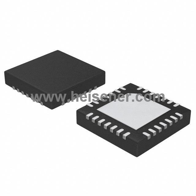
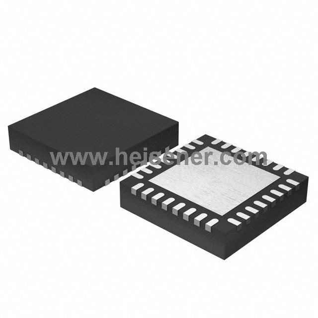
Pin arrangement

IDT5V49EE902 is programmable within the system and can be programmed using the I2C interface. Internal EEPROM allows the user to save and restore the configuration of the device without having to reprogram it at power-on. Each of the four PLLS has a 7-bit reference divider and a 12-bit feedback divider. This allows the user to generate four unique non-integer correlated frequencies.
Characteristics and description of phase locked loop

The PLL bandwidth is programmable, allowing the user to customize the PLL response to the application.For example, users can tune phase-locked loop parameters to minimize jitter generation or maximize jitter attenuation. Spread spectrum generation and/or fractional fractions are allowed on two PLLS. There are a total of six 8-bit output dividers.
Functional Block Diagram

Each output library can be configured to support LVTTL, lvvpecl, LVDS, or HCSL logical levels. Out0 (Output 0) supports only 3.3V single-ended output. The output is connected to the PLL by a switching matrix. The switching matrix allows the user to route PLL outputs to any output group. This feature can be used to simplify and optimize board layout. In addition, the conversion rate and enable/disable functions for each output are programmable.
Test Circuits

Other Termination Scheme (Block Diagram)