| Part Number | FQI47P06TU |
|---|---|
| Manufacturer | Fairchild/ON Semiconductor |
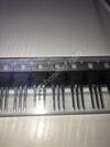
| Description | MOSFET P-CH 60V 47A I2PAK |
| Datasheet | |
| Package | TO-262-3 Long Leads, I2Pak, TO-262AA |
| ECAD |
|
| In Stock | 121,740 piece(s) |
| Unit Price | Request a Quote |
| Lead Time | Can Ship Immediately |
| Estimated Delivery Time | Apr 29 - May 4 (Choose Expedited Shipping) |
| Request for Quotation |
|
| Payment Methods | |
| Delivery Services |
Part Number # FQI47P06TU (Transistors - FETs, MOSFETs - Single) is manufactured by Fairchild/ON Semiconductor and distributed by Heisener. Being one of the leading electronics distributors, we carry many kinds of electronic components from some of the world’s top class manufacturers. Their quality is guaranteed by its stringent quality control to meet all required standards.
For FQI47P06TU specifications/configurations, quotation, lead time, payment terms of further enquiries please have no hesitation to contact us. To process your RFQ, please add FQI47P06TU with quantity into BOM. Heisener.com does NOT require any registration to request a quote of FQI47P06TU.
| Manufacturer | Fairchild/ON Semiconductor |
| Category | Discrete Semiconductor Products - Transistors - FETs, MOSFETs - Single |
| Package | TO-262-3 Long Leads, I2Pak, TO-262AA |
| ECAD |
|
| Series | QFET? |
| FET Type | P-Channel |
| Technology | MOSFET (Metal Oxide) |
| Drain to Source Voltage (Vdss) | 60V |
| Current - Continuous Drain (Id) @ 25°C | 47A (Tc) |
| Drive Voltage (Max Rds On, Min Rds On) | 10V |
| Vgs(th) (Max) @ Id | 4V @ 250µA |
| Gate Charge (Qg) (Max) @ Vgs | 110nC @ 10V |
| Input Capacitance (Ciss) (Max) @ Vds | 3600pF @ 25V |
| Vgs (Max) | ±25V |
| FET Feature | - |
| Power Dissipation (Max) | 3.75W (Ta), 160W (Tc) |
| Rds On (Max) @ Id, Vgs | 26 mOhm @ 23.5A, 10V |
| Operating Temperature | -55°C ~ 175°C (TJ) |
| Mounting Type | Through Hole |
| Supplier Device Package | I2PAK |
| Package / Case | TO-262-3 Long Leads, I2Pak, TO-262AA |
Ele*****Hodge
April 9, 2023
Mos*****Brock
March 10, 2023
Jayla*****phenson
March 2, 2023
Merc*****itaker
March 2, 2023
Hann*****wkins
February 27, 2023


|
VJ0402D100JLXAC | Vishay Vitramon, CAP CER 10PF 25V C0G/NP0 0402, 0402 (1005 Metric), QFET? | View |
 
|
JANTX2N3441 | Microsemi Corporation, TRANS NPN 140V 3A TO-66, TO-213AA, TO-66-2, QFET? | View |

|
X4645S8I-2.7A | Intersil, IC SUPERVISOR CPU 64K EE 8-SOIC, 8-SOIC (0.154", 3.90mm Width), QFET? | View |

|
MAX34561T+ | Maxim Integrated, IC HOT-PLUG SW 12V/5V 24TQFN, 24-WFQFN Exposed Pad, QFET? | View |

|
MB90497GPMC-GS-162-BNDE1 | Cypress Semiconductor Corp, IC MCU 16BIT 64KB MROM 64LQFP, 64-LQFP, QFET? | View |

|
CR0603-FX-4991ELF | Bourns Inc., RES SMD 4.99K OHM 1% 1/10W 0603, 0603 (1608 Metric), QFET? | View |
|
|
TS08015A0000G | Amphenol Anytek, TERM BLOCK PLUG 8POS 7.62MM, -, QFET? | View |
|
|
DWM-26-52-T-D-305 | Samtec Inc., .050" BOARD SPACERS, -, QFET? | View |
|
|
DW-50-11-F-S-650 | Samtec Inc., .025" BOARD SPACERS, -, QFET? | View |

|
1103019-2 | TE Connectivity AMP Connectors, MODULE FEMALE 2+2POS CRIMP, -, QFET? | View |

|
R09P05S/P/R6.4 | Recom Power, CONV DC/DC 1W 09VIN 05VOUT, 7-SIP Module, 4 Leads, QFET? | View |

|
FUSB1500MHX | ON Semiconductor, IC USB 2.0 TRANSCEIVER 16-MLP, 16-WFQFN Exposed Pad, QFET? | View |

We guarantee 100% customer satisfaction.
Our experienced sales team and tech support team back our services to satisfy all our customers.

We provide 90 days warranty.
If the items you received were not in perfect quality, we would be responsible for your refund or replacement, but the items must be returned in their original condition.
| Part Number | Manufacturer | Description | Stock |
FQI47P06TU D# FQI47P06TU |
ON Semiconductor |
MOSFET P-CH 60V 47A I2PAK - Bulk (Alt: FQI47P06TU) RoHS: Compliant
|
0 |
| Part Number | Manufacturer | Description | Stock |
FQI47P06TU |
Fairchild Semiconductor Corporation |
SEMI Date Code: 0705 |
1000 |
| Part Number | Manufacturer | Description | Stock |
FQI47P06TU D# 2156-FQI47P06TU-FS-ND |
Rochester Electronics LLC |
MOSFET P-CH 60V 47A I2PAK |
3979 |
| Part Number | Manufacturer | Description | Stock |
FQI47P06TU |
Rochester Electronics LLC |
OEM/CM QUOTES ONLY | NO BROKERS |
4576 |
| Part Number | Manufacturer | Description | Stock |
FQI47P06TU D# NS-FQI47P06TU |
Fairchild Semiconductor Corporation |
OEM/CM ONLY |
2207 |
| Part Number | Manufacturer | Description | Stock |
FQI47P06TU |
Fairchild Semiconductor Corporation |
47A, 60V, 0.026ohm, P-Channel Power MOSFET, TO-262AA RoHS: Compliant
|
3979 |
| Part Number | Manufacturer | Description | Stock |
FQI47P06TU |
Fairchild Semiconductor Corporation |
OEM/CM ONLY |
2016 |
Heisener's commitment to quality has shaped our processes for sourcing, testing, shipping, and every step in between. This foundation underlies each component we sell.

Do you have any question about FQI47P06TU?
+86-755-83210135-818


Scan to view this page