 0
0


 0
0


Part Number
IRF7493TRPBF
Manufacturer
Description
MOSFET N-CH 80V 9.3A 8-SOIC
Package
8-SOIC (0.154", 3.90mm Width)
In Stock
26,832 piece(s)
Unit Price
Request a Quote
Lead Time
Can Ship Immediately
Estimated Delivery Time
May 23 - May 28 ( Choose Expedited Shipping)
Request for Quotation

Heisener's commitment to quality has shaped our processes for sourcing, testing, shipping, and every step in between. This foundation underlies each component we sell.


Do you have any question about IRF7493TRPBF?

+86-755-83210559 ext. 807


Part Number # IRF7493TRPBF (Transistors - FETs, MOSFETs - Single) is manufactured by Infineon Technologiesand distributed by Heisener. Being one of the leading electronics distributors, we carry many kinds of electronic components from some of the world’s top class manufacturers. Their quality is guaranteed by its stringent quality control to meet all required standards.
For IRF7493TRPBFspecifications/configurations, quotation, lead time, payment terms of further enquiries please have no hesitation to contact us. To process your RFQ, please add IRF7493TRPBF with quantity into BOM. Heisener.com does NOT require any registration to request a quote of IRF7493TRPBF.
Pauli*****ynolds
April 7, 2023
Ryl*****Chang
March 29, 2023
Harl***** Nixon
March 13, 2023
Reig*****unders
March 13, 2023
Scot*****lter
March 4, 2023
Emer*****Murthy
March 3, 2023
Raqu*****yengar
March 1, 2023
Xiom*****Long
February 23, 2023
Mar***** Muni
February 19, 2023
Currently, Heisener only provide peer-to-peer order processing. While you submit the RFQ, our professional agent will contact you with the competitive prices in the global market,
and our agent will prompt you to finish the order if you accept our offers.
We have a professional and experienced quality control team to strictly verify and test theIRF7493TRPBF. All suppliers must pass our qualification reviews before they can publish their products including IRF7493TRPBF on Heisener;we pay more attention to the channels and quality of IRF7493TRPBFproducts than any other customer. We strictly implement supplier audits, so you can purchase with confidence.
3. Are the IRF7493TRPBF price and inventory displayed accurate?The price and inventory of IRF7493TRPBF fluctuates frequently and cannot be updated in time, it will be updated periodically within 24 hours. And, our quotation usually expires after 5 days.
4. What forms of payment are accepted?Wire Transfer, PayPal, Alipay, Wechat, Credit Card, Western Union, MoneyGram, and Escrow are all acceptable.
Warm Tips: Some orders in certain payment forms may require handling fee.
Customers can choose industry-leading freight companies, including DHL, UPS, FedEx, TNT, and Registered Mail. Shipping insurance is also available.
Once your order has been processed for shipment, our salesperson will send you an email advising you of the shipping status and tracking number.
Warm Tips: It may take up to 24 hours for the carriers to display tracking information. Usually, express delivery takes 3-5 days, and registered mail takes 25-60 days.
All goods will implement Pre-Shipment Inspection (PSI), selected at random from all batches of your order to do a systematic inspection before arranging the shipment.
If there is something wrong with the IRF7493TRPBF we delivered, we will accept the replacement or return of the IRF7493TRPBF only when all of the below conditions are fulfilled:
(1)Such as a deficiency in quantity, delivery of wrong items, and apparent external defects (breakage and rust, etc.), and we acknowledge such problems.
(2)We are informed of the defect described above within 90 days after the delivery ofIRF7493TRPBF.
(3)The PartNo is unused and only in the original unpacked packaging.
Two processes to return the products:
(1)Inform us within 90 days
(2)Obtain Requesting Return Authorizations
If you need any after-sales service, please do not hesitate to contact us.


We guarantee 100% customer satisfaction.
Our experienced sales team and tech support team back our services to satisfy all our customers.

We provide 90 days warranty.
If the items you received were not in perfect quality, we would be responsible for your refund or replacement, but the items must be returned in their original condition.

| Part Number | Manufacturer | Description | Stock |
IRF7493TRPBF D# V72:2272_13890867 |
Infineon Technologies AG |
Trans MOSFET N-CH 80V 9.3A 8-Pin SOIC T/R RoHS: Compliant
|
0 |
| Part Number | Manufacturer | Description | Stock |
IRF7493TRPBF D# IRF7493TRPBF |
Infineon Technologies AG |
Trans MOSFET N-CH 80V 9.3A 8-Pin SOIC T/R - Tape and Reel (Alt: IRF7493TRPBF) RoHS: Compliant
|
0 |
| Part Number | Manufacturer | Description | Stock |
IRF7493TRPBF D# SP001575326 |
Infineon Technologies AG |
Trans MOSFET N-CH 80V 9.3A 8-Pin SOIC T/R (Alt: SP001575326) |
0 |
| Part Number | Manufacturer | Description | Stock |
IRF7493TRPBF |
International Rectifier |
Trans MOSFET N-CH 80V 9.3A 8-Pin SOIC T/R |
20000 |
| Part Number | Manufacturer | Description | Stock |
IRF7493TRPBF D# C1S322000485352 |
Infineon Technologies AG |
Trans MOSFET N-CH 80V 9.3A 8-Pin SOIC T/R RoHS: Compliant
pbFree: Yes
Min Qty: 5
Container: Cut Tape
|
3965 |
| Part Number | Manufacturer | Description | Stock |
IRF7493TRPBF |
Infineon Technologies AG |
MOSFET N-CH 80V 9.3A 8-SOIC |
70 |
| Part Number | Manufacturer | Description | Stock |
IRF7493TRPBF D# IRF7493PBFCT-ND |
Infineon Technologies AG |
MOSFET N-CH 80V 9.3A 8SO |
11643 |
| Part Number | Manufacturer | Description | Stock |
IRF7493TRPBF D# 2725911RL |
Infineon Technologies AG |
MOSFET, N-CH, 80V, 9.3A, SOIC RoHS: Compliant
Min Qty: 1
Container: Reel
|
0 |
| Part Number | Manufacturer | Description | Stock |
IRF7493TRPBF |
Infineon Technologies AG |
Single N-Channel 80 V 15 mOhm 53 nC HEXFET® Power Mosfet - SOIC-8 RoHS: Compliant
pbFree: Yes
|
8000 |
| Part Number | Manufacturer | Description | Stock |
IRF7493TRPBF |
IOR |
OEM/CM QUOTES ONLY | NO BROKERS |
46400 |
| Part Number | Manufacturer | Description | Stock |
IRF7493TRPBF |
Infineon Technologies AG |
N-Channel 9.3A (Tc) 2.5W (Tc) Surface Mount 8-SO RoHS: Compliant
|
24178 |
| Part Number | Manufacturer | Description | Stock |
IRF7493TRPBF D# C13914 |
Infineon Technologies AG | 4593 |
| Part Number | Manufacturer | Description | Stock |
IRF7493TRPBF |
International Rectifier |
OEM/CM Immediate delivery |
8800000 |
| Part Number | Manufacturer | Description | Stock |
IRF7493TRPBF D# 942-IRF7493TRPBF |
Infineon Technologies AG |
MOSFET MOSFT 80V 9.2A 15mOhm 31nC Qg RoHS: Compliant
|
2926 |
| Part Number | Manufacturer | Description | Stock |
IRF7493TRPBF D# IRF7493TRPBF |
International Rectifier |
Power Field-Effect Transistor, 17AI(D),100V,0.09ohm, 1-Element, N-Channel,Silicon,Metal-oxideSemiconductor FET |
33950 |
| Part Number | Manufacturer | Description | Stock |
IRF7493TRPBF D# 13AC9202 |
Infineon Technologies AG |
MOSFET, N-CH, 80V, 9.3A, SOIC, Transistor Polarity:N Channel, Continuous Drain Current Id:9.3A, Drain Source Voltage Vds:80V, On Resistance Rds(on):0.0115ohm, Rds(on) Test Voltage Vgs:10V, Threshold Voltage Vgs:4V, Power Dissipation RoHS Compliant: Yes RoHS: Compliant
Min Qty: 1
Container: Cut Tape
|
0 |
| Part Number | Manufacturer | Description | Stock |
IRF7493TRPBF D# NS-IRF7493TRPBF |
International Rectifier |
OEM/CM ONLY |
7528 |
| Part Number | Manufacturer | Description | Stock |
IRF7493TRPBF |
International Rectifier |
9.3 A, 80 V, 0.015 OHM, N-CHANNEL, SI, POWER, MOSFET, MS-012AA, TandR, LEAD FREE |
132 |
| Part Number | Manufacturer | Description | Stock |
IRF7493TRPBF D# 9154960P |
Infineon Technologies AG |
N-Channel MOSFET, 9.3 A, 80 V, 8-Pin SOIC Infineon IRF7493TRPBF, RL Min Qty: 10
Container: Reel
|
480 |
| Part Number | Manufacturer | Description | Stock |
IRF7493TRPBF D# TMOSP11961 |
Infineon Technologies AG |
N-CH 80V 9,2A 15mOhm SO8 RoHS: Compliant
|
0 |
| Part Number | Manufacturer | Description | Stock |
IRF7493TRPBF |
International Rectifier |
OEM/CM ONLY |
52742 |
| Part Number | Manufacturer | Description | Stock |
IRF7493TRPBF |
International Rectifier |
IN stock Immediate delivery |
8799985 |
| Part Number | Manufacturer | Description | Stock |
IRF7493TRPBF |
International Rectifier |
shipping today |
11996 |
| Part Number | Manufacturer | Description | Stock |
IRF7493TRPBF D# 36466852 |
Infineon Technologies AG |
Trans MOSFET N-CH 80V 9.3A 8-Pin SOIC T/R RoHS: Compliant
|
0 |
| Part Number | Manufacturer | Description | Stock |
IRF7493TRPBF |
International Rectifier |
RFQ |
469 |
| Part Number | Manufacturer | Description | Stock |
IRF7493TRPBF |
Infineon Technologies AG |
MOSFET N-CH 80V 9.3A 8-SOIC |
12805 |
| Part Number | Manufacturer | Description | Stock |
IRF7493TRPBF D# 2725911 |
Infineon Technologies AG |
MOSFET, N-CH, 80V, 9.3A, SOIC RoHS: Compliant
Min Qty: 1
Container: Cut Tape
|
97 |


IC DAC VIDEO 3CH 170MHZ 48LQFP
DIODE ZENER 3.6V 500MW SOD123
DGTL ISO 2.5KV GEN PURP 16SOIC

IC FLASH 512MBIT 100NS 56TSOP
IC MULTIPLIER 4-QUADRANT 8-SOIC

IC COMPARATOR DUAL LP 8-SOIC
IC SDRAM 2GBIT 800MHZ 96BGA
DIODE ZENER 5.1V 225MW SOT23-3

RF TXRX MODULE BLUETOOTH U.FL

IC LATCH 8BIT ADDRESS 16-SOIC


SIT8209AC-33-28S-125.000000Y
SiTime, -20 TO 70C, 5032, 50PPM, 2.8V, 1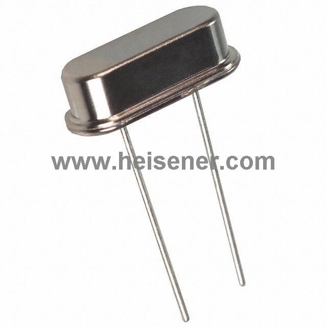
ATS037A
CTS-Frequency Controls, CRYSTAL 3.6864MHZ SERIES T/H
MCP6N11T-001E/SN
Microchip Technology, IC OPAMP INSTR 500KHZ RRO 8SOIC
MXLPLAD15KP130CAE3
Microsemi Corporation, TVS DIODE 130VWM 209VC PLAD
06631.25HXSL
Littelfuse Inc., FUSE BRD MNT 1.25A 250VAC RADIAL
RWR81S7R00FRBSL
Vishay Dale, RES 7 OHM 1W 1% WW AXIAL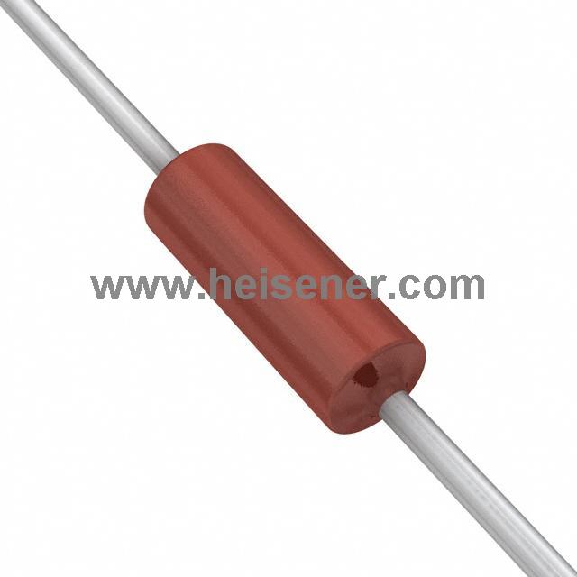
CMF5518K700FHEK
Vishay Dale, RES 18.7K OHM 1/2W 1% AXIAL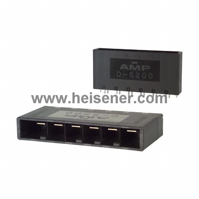
1-179960-3
TE Connectivity AMP Connectors, CONN HEADER 6POS KEY-X 30GOLD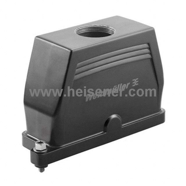
1082870000
Weidmuller, CONN HOOD TOP ENTRY SZ8 M40
FGG.2B.302.CLAD72Z
LEMO, CONN INLINE PLUG 2PIN SLD CUP
0459851231
Molex, LLC, CONN HEADER 10PWR 20SGL 3.18MM
AP7311-28SNG-7
Diodes Incorporated, IC REG LINEAR 2.8V 150MA