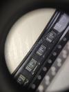
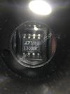
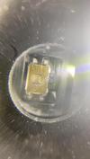
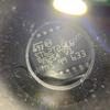
| Part Number | IRL3705NPBF |
|---|---|
| Manufacturer | Infineon Technologies |
| Description | MOSFET N-CH 55V 89A TO-220AB |
| Datasheet | |
| Package | TO-220-3 |
| ECAD |
|
| In Stock | 48,756 piece(s) |
| Unit Price | Request a Quote |
| Lead Time | Can Ship Immediately |
| Estimated Delivery Time | Apr 28 - May 3 (Choose Expedited Shipping) |
| Request for Quotation |
|
| Payment Methods | |
| Delivery Services |
Part Number # IRL3705NPBF (Transistors - FETs, MOSFETs - Single) is manufactured by Infineon Technologies and distributed by Heisener. Being one of the leading electronics distributors, we carry many kinds of electronic components from some of the world’s top class manufacturers. Their quality is guaranteed by its stringent quality control to meet all required standards.
For IRL3705NPBF specifications/configurations, quotation, lead time, payment terms of further enquiries please have no hesitation to contact us. To process your RFQ, please add IRL3705NPBF with quantity into BOM. Heisener.com does NOT require any registration to request a quote of IRL3705NPBF.
| Manufacturer | Infineon Technologies |
| Category | Discrete Semiconductor Products - Transistors - FETs, MOSFETs - Single |
| Package | TO-220-3 |
| ECAD |
|
| Series | HEXFET? |
| FET Type | N-Channel |
| Technology | MOSFET (Metal Oxide) |
| Drain to Source Voltage (Vdss) | 55V |
| Current - Continuous Drain (Id) @ 25°C | 89A (Tc) |
| Drive Voltage (Max Rds On, Min Rds On) | 4V, 10V |
| Vgs(th) (Max) @ Id | 2V @ 250µA |
| Gate Charge (Qg) (Max) @ Vgs | 98nC @ 5V |
| Input Capacitance (Ciss) (Max) @ Vds | 3600pF @ 25V |
| Vgs (Max) | ±16V |
| FET Feature | - |
| Power Dissipation (Max) | 170W (Tc) |
| Rds On (Max) @ Id, Vgs | 10 mOhm @ 46A, 10V |
| Operating Temperature | -55°C ~ 175°C (TJ) |
| Mounting Type | Through Hole |
| Supplier Device Package | TO-220AB |
| Package / Case | TO-220-3 |
Alic*****ynes
March 22, 2023
Andr*****unshi
March 19, 2023
Aly***** Dash
March 15, 2023
Mada***** Kirby
March 10, 2023
Lawso*****nnell
March 4, 2023
Victo*****allick
February 23, 2023


|
TH3B156M025D1400 | Vishay Sprague, CAP TANT 15UF 25V 20% 1411, 1411 (3528 Metric), HEXFET? | View |

|
GRM0336S1E100JD01D | Murata, CAP CER 10PF 25V S2H 0201, 0201 (0603 Metric), HEXFET? | View |
|
|
1812Y1K20822MXR | Knowles Syfer, CAP CER 8200PF 1.2KV X7R 1812, 1812 (4532 Metric), HEXFET? | View |

|
SST39VF802C-70-4C-MAQE-T | Microchip Technology, IC FLASH 8MBIT 70NS 48WFBGA, 48-WFBGA, HEXFET? | View |
 
|
LMP90077MHX/NOPB | Texas Instruments, IC AFE 16BIT 214.6SPS 28TSSOP, 28-TSSOP (0.173", 4.40mm Width) Exposed Pad, HEXFET? | View |

|
RN55D1581FBSL | Vishay Dale, RES 1.58K OHM 1/8W 1% AXIAL, Axial, HEXFET? | View |
|
|
0438100276 | Molex, LLC, MF SMC RA HDR W/O CLIP GOLD, -, HEXFET? | View |
|
|
951410-4011309-AR-PT | 3M, CONN HDR STR STACK 10POS 2MM SMD, -, HEXFET? | View |
|
|
CA06COMPG24-28SB | ITT Cannon, LLC, CONN PLUG 24POS INLINE W/SKTS, -, HEXFET? | View |
|
|
TV07DT-17-2P | Amphenol Aerospace Operations, CONN RCPT MALE 39POS GOLD CRIMP, -, HEXFET? | View |
|
|
CA06COMPG14S-2S | ITT Cannon, LLC, CONN PLUG 4POS INLINE W/SKTS, -, HEXFET? | View |
|
|
AIT6UW28-3SWS | Amphenol Industrial Operations, ER 3C 3#8 SKT PLUG, -, HEXFET? | View |

We guarantee 100% customer satisfaction.
Our experienced sales team and tech support team back our services to satisfy all our customers.

We provide 90 days warranty.
If the items you received were not in perfect quality, we would be responsible for your refund or replacement, but the items must be returned in their original condition.
| Part Number | Manufacturer | Description | Stock |
IRL3705NPBF D# V99:2348_13892831 |
Infineon Technologies AG |
Trans MOSFET N-CH 55V 89A 3-Pin(3+Tab) TO-220AB Tube |
0 |
| Part Number | Manufacturer | Description | Stock |
IRL3705NPBF D# IRL3705NPBF |
Infineon Technologies AG |
Trans MOSFET N-CH 55V 89A 3-Pin(3+Tab) TO-220AB T/R - Bulk (Alt: IRL3705NPBF) RoHS: Compliant
|
0 |
| Part Number | Manufacturer | Description | Stock |
IRL3705NPBF D# SP001578520 |
Infineon Technologies AG |
Trans MOSFET N-CH 55V 89A 3-Pin(3+Tab) TO-220AB T/R (Alt: SP001578520) |
0 |
| Part Number | Manufacturer | Description | Stock |
IRL3705NPBF |
International Rectifier |
Min Qty 150 |
5650 |
| Part Number | Manufacturer | Description | Stock |
IRL3705NPBF |
Infineon Technologies AG |
N-Channel 55V 89A 2V @ 250uA 10mohms @ 46A,10V 170W TO-220(TO-220-3) MOSFET RoHS |
81 |
| Part Number | Manufacturer | Description | Stock |
IRL3705NPBF D# IRL3705NPBF-ND |
Infineon Technologies AG |
MOSFET N-CH 55V 89A TO220AB |
1292 |
| Part Number | Manufacturer | Description | Stock |
IRL3705NPBF |
International Rectifier |
In stock shipping within 2days |
5805 |
| Part Number | Manufacturer | Description | Stock |
IRL3705NPBF D# 8651019 |
Infineon Technologies AG |
MOSFET, N, 55V, 77A, TO-220 RoHS: Compliant
Min Qty: 1
Container: Each
|
98 |
| Part Number | Manufacturer | Description | Stock |
IRL3705NPBF |
Infineon Technologies AG |
Single N-Channel 55 V 0.012 Ohm 98 nC HEXFET® Power Mosfet - TO-220-3 RoHS: Compliant
pbFree: Yes
|
0 |
| Part Number | Manufacturer | Description | Stock |
IRL3705NPBF |
Infineon Technologies AG |
OEM/CM QUOTES ONLY | NO BROKERS |
11600 |
| Part Number | Manufacturer | Description | Stock |
IRL3705NPBF D# C2667 |
Infineon Technologies AG | 78 |
| Part Number | Manufacturer | Description | Stock |
IRL3705NPBF |
International Rectifier |
OEM/CM Immediate delivery |
10000 |
| Part Number | Manufacturer | Description | Stock |
IRL3705NPBF D# 942-IRL3705NPBF |
Infineon Technologies AG |
MOSFET MOSFT 55V 77A 65.3nC 10mOhm LogLvAB RoHS: Compliant
|
1020 |
| Part Number | Manufacturer | Description | Stock |
IRL3705NPBF D# XSKDRABV0033197 |
Infineon Technologies AG |
55V Single N-Channel HEXFET Power MOSFET in a TO-220AB package |
24950 |
| Part Number | Manufacturer | Description | Stock |
IRL3705NPBF D# 38K3057 |
Infineon Technologies AG |
TRANSISTOR MOSFETS ROHS COMPLIANT: YES RoHS: Compliant
Min Qty: 1
Container: Bulk
|
240 |
| Part Number | Manufacturer | Description | Stock |
IRL3705NPBF D# NS-IRL3705NPBF |
International Rectifier |
OEM/CM ONLY |
1108 |
| Part Number | Manufacturer | Description | Stock |
IRL3705NPBF D# 5409991 |
Infineon Technologies AG |
N-Channel MOSFET, 89 A, 55 V, 3-Pin TO-220AB Infineon IRL3705NPBF, EA Min Qty: 1
Container: Bulk
|
396 |
| Part Number | Manufacturer | Description | Stock |
IRL3705NPBF |
Infineon Technologies AG |
IRL3705 - 12V-300V N-Channel Power MOSFET RoHS: Compliant
|
924 |
| Part Number | Manufacturer | Description | Stock |
IRL3705NPBF |
International Rectifier |
OEM/CM ONLY |
5424 |
| Part Number | Manufacturer | Description | Stock |
IRL3705NPBF |
International Rectifier |
IN stock Immediate delivery |
10015 |
| Part Number | Manufacturer | Description | Stock |
IRL3705NPBF C |
International Rectifier |
shipping today |
25776 |
IRL3705NPBF |
International Rectifier |
shipping today |
34996 |
| Part Number | Manufacturer | Description | Stock |
IRL3705NPBF D# 53149995 |
Infineon Technologies AG |
Trans MOSFET N-CH 55V 89A 3-Pin(3+Tab) TO-220AB Tube |
0 |
| Part Number | Manufacturer | Description | Stock |
IRL3705NPBF |
mfr |
RFQ |
14422 |
| Part Number | Manufacturer | Description | Stock |
IRL3705NPBF |
Infineon Technologies AG |
MOSFET N-CH 55V 89A TO-220AB |
846 |
| Part Number | Manufacturer | Description | Stock |
IRL3705NPBF D# 8651019 |
Infineon Technologies AG |
MOSFET, N, 55V, 77A, TO-220 RoHS: Compliant
Min Qty: 1
Container: Each
|
98 |
Heisener's commitment to quality has shaped our processes for sourcing, testing, shipping, and every step in between. This foundation underlies each component we sell.

Do you have any question about IRL3705NPBF?
86-755-83210559-843


Scan to view this page