| Part Number | IXTT52N30P |
|---|---|
| Manufacturer | IXYS |
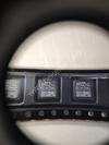
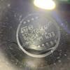
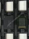
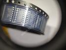
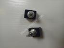
| Description | MOSFET N-CH 300V 52A TO-268 |
| Datasheet | |
| Package | TO-268-3, D3Pak (2 Leads + Tab), TO-268AA |
| ECAD |
|
| In Stock | 5,808 piece(s) |
| Unit Price | Request a Quote |
| Lead Time | Can Ship Immediately |
| Estimated Delivery Time | Apr 29 - May 4 (Choose Expedited Shipping) |
| Request for Quotation |
|
| Payment Methods | |
| Delivery Services |
Part Number # IXTT52N30P (Transistors - FETs, MOSFETs - Single) is manufactured by IXYS and distributed by Heisener. Being one of the leading electronics distributors, we carry many kinds of electronic components from some of the world’s top class manufacturers. Their quality is guaranteed by its stringent quality control to meet all required standards.
For IXTT52N30P specifications/configurations, quotation, lead time, payment terms of further enquiries please have no hesitation to contact us. To process your RFQ, please add IXTT52N30P with quantity into BOM. Heisener.com does NOT require any registration to request a quote of IXTT52N30P.
| Manufacturer | IXYS |
| Category | Discrete Semiconductor Products - Transistors - FETs, MOSFETs - Single |
| Package | TO-268-3, D3Pak (2 Leads + Tab), TO-268AA |
| ECAD |
|
| Series | PolarHT? |
| FET Type | N-Channel |
| Technology | MOSFET (Metal Oxide) |
| Drain to Source Voltage (Vdss) | 300V |
| Current - Continuous Drain (Id) @ 25°C | 52A (Tc) |
| Drive Voltage (Max Rds On, Min Rds On) | 10V |
| Vgs(th) (Max) @ Id | 5V @ 250µA |
| Gate Charge (Qg) (Max) @ Vgs | 110nC @ 10V |
| Input Capacitance (Ciss) (Max) @ Vds | 3490pF @ 25V |
| Vgs (Max) | ±20V |
| FET Feature | - |
| Power Dissipation (Max) | 400W (Tc) |
| Rds On (Max) @ Id, Vgs | 66 mOhm @ 500mA, 10V |
| Operating Temperature | -55°C ~ 150°C (TJ) |
| Mounting Type | Surface Mount |
| Supplier Device Package | TO-268 |
| Package / Case | TO-268-3, D3Pak (2 Leads + Tab), TO-268AA |
Rene*****lkarni
March 31, 2023
Gustav*****amaniam
March 29, 2023
Augus*****treras
March 27, 2023
Amo*****otter
March 24, 2023
Isabe*****antana
March 23, 2023
Bro*****Dyer
March 16, 2023
Bret*****ickson
March 1, 2023
Daws*****earson
February 23, 2023


|
0603Y0160680KCT | Knowles Syfer, CAP CER 68PF 16V C0G/NP0 0603, 0603 (1608 Metric), PolarHT? | View |

|
70T3339S133BFI8 | IDT, Integrated Device Technology Inc, IC SRAM 9MBIT 133MHZ 208CABGA, 208-LFBGA, PolarHT? | View |

|
BK1/S500-50-R | Eaton, FUSE GLASS 50MA 250VAC 5X20MM, 5mm x 20mm, PolarHT? | View |

|
7213J37ZBI22 | C&K, SWITCH ROCKER SP3T 0.4VA 20V, -, PolarHT? | View |

|
TNPW12063K48BEEA | Vishay Dale, RES SMD 3.48K OHM 0.1% 1/4W 1206, 1206 (3216 Metric), PolarHT? | View |

|
RC5025J470CS | Samsung, RES SMD 47 OHM 5% 2/3W 2010, 2010 (5025 Metric), PolarHT? | View |
|
|
FTM-125-02-L-DV-SA | Samtec Inc., 1MM MICRO STRIPS, -, PolarHT? | View |
|
|
PC06P-22-36S | Amphenol Industrial Operations, CONN PLUG 36POS INLINE SKT, -, PolarHT? | View |
|
|
MS3475L20-16PX | Amphenol Aerospace Operations, CONN PLUG 16POS INLINE PIN, -, PolarHT? | View |
|
|
GBB64DHRR | Sullins Connector Solutions, CONN EDGE DUAL FMALE 128POS .050, -, PolarHT? | View |
|
|
ECC30DRYI | Sullins Connector Solutions, CONN EDGE DUAL FMALE 60POS 0.100, -, PolarHT? | View |
|
|
VI-B1D-CU-B1 | Vicor Corporation, CONVERTER MOD DC/DC 85V 200W, Full Brick, PolarHT? | View |

We guarantee 100% customer satisfaction.
Our experienced sales team and tech support team back our services to satisfy all our customers.

We provide 90 days warranty.
If the items you received were not in perfect quality, we would be responsible for your refund or replacement, but the items must be returned in their original condition.
| Part Number | Manufacturer | Description | Stock |
IXTT52N30P D# V36:1790_15877569 |
Littelfuse Inc |
Trans MOSFET N-CH 300V 52A 3-Pin(2+Tab) TO-268 |
0 |
| Part Number | Manufacturer | Description | Stock |
IXTT52N30P |
IXYS Corporation |
MOSFET N-CH 300V 52A TO-268 |
0 |
| Part Number | Manufacturer | Description | Stock |
IXTT52N30P D# IXTT52N30P-ND |
IXYS Corporation |
MOSFET N-CH 300V 52A TO268 |
0 |
| Part Number | Manufacturer | Description | Stock |
IXTT52N30P |
IXYS Corporation |
OEM/CM QUOTES ONLY | NO BROKERS |
3898 |
| Part Number | Manufacturer | Description | Stock |
IXTT52N30P D# 03AH1848 |
Littelfuse Inc |
DISC MOSFET N-CH STD-POLAR TO-268AA / TUBE RoHS: Not Compliant
Min Qty: 300
Container: Bulk
|
0 |
| Part Number | Manufacturer | Description | Stock |
IXTT52N30P D# NS-IXTT52N30P |
IXYS Corporation |
OEM/CM ONLY |
4522 |
| Part Number | Manufacturer | Description | Stock |
IXTT52N30P |
IXYS Corporation |
MOSFET 52 Amps 300V 0.066 Rds pbFree: Pb-Free
|
0 |
Heisener's commitment to quality has shaped our processes for sourcing, testing, shipping, and every step in between. This foundation underlies each component we sell.

Do you have any question about IXTT52N30P?
+86-755-83210559-834


Scan to view this page