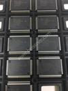
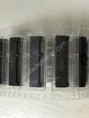
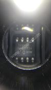
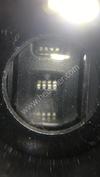
Page 1
Page 2
General Description
The MAX7315 I2C-/SMBus-compatible serial interfaced
peripheral provides microprocessors with 8 I/O ports.
Each I/O port can be individually configured as either an
open-drain current-sinking output rated at 50mA at 5.5V,
or a logic input with transition detection. A ninth port can
be used for transition detection interrupt or as a general-
purpose output. The outputs are capable of directly dri-
ving LEDs, or providing logic outputs with external
resistive pullup up to 5.5V.
PWM current drive is integrated with 8 bits of control.
Four bits are global control and apply to all LED outputs
to provide coarse adjustment of current from fully off to
fully on in 14 intensity steps. Each output then has indi-
vidual 4-bit control, which further divides the globally
set current into 16 more steps. Alternatively, the current
control can be configured as a single 8-bit control that
sets all outputs at once.
The MAX7315 is pin and software compatible with the
PCA9534 and PCA9554(A).
Each output has independent blink timing with two blink
phases. All LEDs can be individually set to be on or off
during either blink phase, or to ignore the blink control.
The blink period is controlled by a register.
The MAX7315 supports hot insertion. All port pins, the INT
output, SDA, SCL, and the slave address inputs ADO-2
remain high impedance in power-down (V+ = 0V) with up
to 6V asserted upon them.
The MAX7315 is controlled through the 2-wire I2C/SMBus
serial interface, and can be configured to one of 64 I2C
addresses.
Applications
Features
© 400kbps, 2-Wire Serial Interface, 5.5V Tolerant
© 2V to 3.6V Operation
© Overall 8-Bit PWM LED Intensity Control
Global 16-Step Intensity Control
Plus Individual 16-Step Intensity Control
© Automatic Two-Phase LED Blinking
© 50mA Maximum Port Output Current
© Supports Hot Insertion
© Outputs Are 5.5V-Rated Open Drain
© Inputs Are Overvoltage Protected to 5.5V
© Transition Detection with Interrupt Output
© Low Standby Current (1.2µA typ; 3.3µA max)
© Tiny 3mm x 3mm, Thin QFN Package
© -40°C to +125°C Temperature Range
© All Ports Can Be Configured as Inputs or Outputs
M
A
X
7
3
1
5
8-Port I/O Expander with LED Intensity
Control, Interrupt, and Hot-Insertion Protection
________________________________________________________________ Maxim Integrated Products 1
12 11 10 9
IN
T
/O
8
P
7
P
6
5
6
7
8
P3
GND
P5
16
15
14
13
AD1
ADO
V+
1 2 3 4
A
D
2
P
0
P
1
P
2
SDA
P4
S
C
L
THIN QFN
TOP VIEW
MAX7315ATE
Pin Configurations
19-3056; Rev 3; 1/05
For pricing, delivery, and ordering information, please contact Maxim/Dallas Direct! at
1-888-629-4642, or visit Maxim’s website at www.maxim-ic.com.
EVALU
ATION
KIT
AVAILA
BLE
Ordering Information
PART
TEMP
RANGE
PIN-
PACKAGE
TOP
MARK
PKG
CODE
MAX7315ATE -40°C to +125°C
16 Thin QFN
3mm x 3mm
x 0.8mm
AAU T1633-4
MAX7315AEE -40°C to +125°C 16 QSOP — —
MAX 7315AU E -40°C to +125°C 16 TSSOP — —
Pin Configurations continued at end of data sheet.
LCD Backlights
LED Status Indication
Portable Equipment
Laptop Computers
Keypad Backlights
RGB LED Drivers
Cellular Phones
Typical Application Circuit appears at end of data sheet.
Page 3
M
A
X
7
3
1
5
8-Port I/O Expander with LED Intensity
Control, Interrupt, and Hot-Insertion Protection
2 _______________________________________________________________________________________
ABSOLUTE MAXIMUM RATINGS
Stresses beyond those listed under “Absolute Maximum Ratings” may cause permanent damage to the device. These are stress ratings only, and functional
operation of the device at these or any other conditions beyond those indicated in the operational sections of the specifications is not implied. Exposure to
absolute maximum rating conditions for extended periods may affect device reliability.
Voltage (with respect to GND)
V+ .............................................................................-0.3V to +4V
SCL, SDA, AD0, AD1, AD2, P0–P7 ..........................-0.3V to +6V
INT/O8 .....................................................................-0.3V to +8V
DC Current on P0–P7, INT/O8 ............................................55mA
DC Current on SDA.............................................................10mA
Maximum GND Current ....................................................190mA
Continuous Power Dissipation (TA = +70°C)
16-Pin TSSOP (derate 9.4mW/°C over +70°C) ............754mW
16-Pin QSOP (derate 8.3mW/°C over +70°C)..............666mW
16-Pin QFN (derate 14.7mW/°C over +70°C) ............1176mW
Operating Temperature Range (TMIN to TMAX)-40°C to +125°C
Junction Temperature ......................................................+150°C
Storage Temperature Range .............................-65°C to +150°C
Lead Temperature (soldering, 10s) .................................+300°C
ELECTRICAL CHARACTERISTICS
(Typical Operating Circuit, V+ = 2V to 3.6V, TA = TMIN to TMAX, unless otherwise noted. Typical values are at V+ = 3.3V, TA = +25°C.)
(Note 1)
PARAMETER SYMBOL CONDITIONS MIN TYP MAX UNITS
Operating Supply Voltage V+ 2 3.6 V
Output Load External Supply
Voltage
VEXT 0 5.5 V
TA = +25°C 1.2 2.3
TA = -40°C to +85°C 2.6
Standby Current
(Interface Idle, PWM Disabled)
I+
SCL and SDA at V +; other
digital inp uts at V + or GN D;
PWM intensi ty contr ol disab led TA = TMIN to TMAX 3.3
µA
TA = +25°C 7 12.1
TA = -40°C to +85°C 13.5
Supply Current
(Interface Idle, PWM Enabled)
I+
SCL and SDA at V +; other
digital inp uts at V + or GN D;
PWM intensi ty contr ol enab led TA = TMIN to TMAX 14.4
µA
TA = +25°C 40 76
TA = -40°C to +85°C 78
Supply Current
(Interface Running, PWM
Disabled)
I+
fSCL = 400kHz; other digital
inputs at V+ or GND; PWM
intensity control disabled TA = TMIN to TMAX 80
µA
TA = +25°C 51 110
TA = -40°C to +85°C 117
Supply Current
(Interface Running, PWM
Enabled)
I+
fSCL = 400kHz; other digital
inputs at V+ or GND; PWM
intensity control enabled TA = TMIN to TMAX 122
µA
Input High Voltage
SDA, SCL, AD0, AD1, AD2,
P0–P7
VIH
0.7 5
V+
V
Input Low Voltage
SDA, SCL, AD0, AD1, AD2,
P0–P7
VIL
0.3 5
V+
V
Input Leakage Current
SDA, SCL, AD0, AD1, AD2,
P0–P7
IIH, IIL Input = GND or V+ -0.2 +0.2 µA
Input Capacitance
SDA, SCL, AD0, AD1, AD2,
P0–P7
8 pF
Page 4
M
A
X
7
3
1
5
8-Port I/O Expander with LED Intensity
Control, Interrupt, and Hot-Insertion Protection
_______________________________________________________________________________________ 3
ELECTRICAL CHARACTERISTICS (continued)
(Typical Operating Circuit, V+ = 2V to 3.6V, TA = TMIN to TMAX, unless otherwise noted. Typical values are at V+ = 3.3V, TA= + 25°C.)
(Note 1)
PARAMETER SYMBOL CONDITIONS MIN TYP MAX UNITS
TA = +25°C 0.15 0.25
TA = -40°C to +85°C 0.29V+ = 2V, ISINK = 20mA
TA = TMIN to TMAX 0.31
TA = +25°C 0.13 0.22
TA = -40°C to +85°C 0.25V+ = 2.5V, ISINK = 20mA
TA = TMIN to TMAX 0.27
TA = +25°C 0.12 0.22
TA = -40°C to +85°C 0.23
Output Low Voltage
P0–P7, INT/O8
VOL
V+ = 3.3V, ISINK = 20mA
TA = TMIN to TMAX 0.25
V
Output Low-Voltage SDA VOLSDA ISINK = 6mA 0.4 V
PWM Clock Frequency fPWM 32 kHz
TIMING CHARACTERISTICS
(Typical Operating Circuit, V+ = 2V to 3.6V, TA = TMIN to TMAX, unless otherwise noted. Typical values are at V+ = 3.3V, TA = +25°C.)
(Note 1)
PARAMETER SYMBOL CONDITIONS MIN TYP MAX UNITS
Serial Clock Frequency fSCL 400 kHz
Bus Free Time Between a STOP and a START
Condition
tBUF 1.3 µs
Hold Time, Repeated START Condition tHD, STA 0.6 µs
Repeated START Condition Setup Time tSU, STA 0.6 µs
STOP Condition Setup Time tSU, STO 0.6 µs
Data Hold Time tHD, DAT (Note 2) 0.9 µs
Data Setup Time tSU, DAT 180 ns
SCL Clock Low Period tLOW 1.3 µs
SCL Clock High Period tHIGH 0.7 µs
Rise Time of Both SDA and SCL Signals, Receiving tR (Notes 3, 4)
200 +
0.1Cb
300 ns
Fall Time of Both SDA and SCL Signals, Receiving tF (Notes 3, 4)
200 +
0.1Cb
300 ns
Fall Time of SDA Transmitting tF.TX (Notes 3, 5)
200 +
0.1Cb
250 ns
Pulse Width of Spike Suppressed tSP (Note 6) 50 ns
Capacitive Load for Each Bus Line Cb (Note 3) 400 pF
Page 5
M
A
X
7
3
1
5
8-Port I/O Expander with LED Intensity
Control, Interrupt, and Hot-Insertion Protection
4 _______________________________________________________________________________________
TIMING CHARACTERISTICS (continued)
(Typical Operating Circuit, V+ = 2V to 3.6V, TA = TMIN to TMAX, unless otherwise noted. Typical values are at V+ = 3.3V, TA = +25°C.)
(Note 1)
PARAMETER SYMBOL CONDITIONS MIN TYP MAX UNITS
Interrupt Valid tIV Figure 10 6.5 µs
Interrupt Reset tIR Figure 10 1 µs
Output Data Valid tDV Figure 10 5 µs
Input Data Setup Time tDS Figure 10 100 ns
Input Data Hold Time tDH Figure 10 1 µs
Note 1: All parameters tested at TA = +25°C. Specifications over temperature are guaranteed by design.
Note 2: A master device must provide a hold time of at least 300ns for the SDA signal (referred to VIL of the SCL signal) to bridge
the undefined region of SCL’s falling edge.
Note 3: Guaranteed by design.
Note 4: Cb = total capacitance of one bus line in pF. tR and tF measured between 0.3 x VDD and 0.7 x VDD.
Note 5: ISINK ≤ 6mA. Cb = total capacitance of one bus line in pF. tR and tF measured between 0.3 x VDD and 0.7 x VDD.
Note 6: Input filters on the SDA and SCL inputs suppress noise spikes less than 50ns.
STANDBY CURRENT vs. TEMPERATURE
M
A
X
7
3
1
5
to
c
0
1
TEMPERATURE (°C)
S
T
A
N
D
B
Y
C
U
R
R
E
N
T
(µ
A
)
1109565 80-10 5 20 35 50-25
1
2
3
4
5
6
7
8
9
10
0
-40 125
V+ = 3.6V
PWM ENABLED
V+ = 2.7V
PWM ENABLED
V+ = 2V
PWM DISABLED
V+ = 2.7V
PWM DISABLED
V+ = 3.6V
PWM
DISABLED
V+ = 2V
PWM ENABLED
SUPPLY CURRENT vs. TEMPERATURE
(PWM DISABLED; fSCL = 400kHz)
M
A
X
7
3
1
5
to
c
0
2
TEMPERATURE (°C)
S
U
P
P
L
Y
C
U
R
R
E
N
T
(µ
A
)
1109565 80-10 5 20 35 50-25
10
20
30
40
50
60
70
0
-40 125
V+ = 3.6V
V+ = 2.7V
V+ = 2V
5
10
15
20
25
30
35
40
45
50
55
60
65
70
0
SUPPLY CURRENT vs. TEMPERATURE
(PWM ENABLED; fSCL = 400kHz)
M
A
X
7
3
1
5
to
c
0
3
TEMPERATURE (°C)
S
U
P
P
L
Y
C
U
R
R
E
N
T
(µ
A
)
1109565 80-10 5 20 35 50-25-40 125
V+ = 3.6V
V+ = 2.7V
V+ = 2V
__________________________________________Typical Operating Characteristics
(TA = +25°C, unless otherwise noted.)
Page 6
M
A
X
7
3
1
5
8-Port I/O Expander with LED Intensity
Control, Interrupt, and Hot-Insertion Protection
_______________________________________________________________________________________ 5
PORT OUTPUT LOW VOLTAGE WITH 50mA
LOAD CURRENT vs. TEMPERATURE
P
O
R
T
O
U
T
P
U
T
L
O
W
V
O
L
T
A
G
E
V
O
L
(V
)
0.1
0.2
0.3
0.4
0.5
0.6
0
M
A
X
7
3
1
5
to
c
0
4
TEMPERATURE (°C)
1109565 80-10 5 20 35 50-25-40 125
V+ = 3.6V
V+ = 2.7V
V+ = 2V
PORT OUTPUT LOW VOLTAGE WITH 20mA
LOAD CURRENT vs. TEMPERATURE
M
A
X
7
3
1
5
to
c
0
5
TEMPERATURE (°C)
P
O
R
T
O
U
T
P
U
T
L
O
W
V
O
L
T
A
G
E
V
O
L
(V
)
1109580655035205-10-25
0.1
0.2
0.3
0.4
0.5
0.6
0
-40 125
ALL OUTPUTS LOADED
V+ = 3.6VV+ = 2.7V
V+ = 2V
PWM CLOCK FREQUENCY
vs. TEMPERATURE
M
A
X
7
3
1
5
to
c
0
6
TEMPERATURE (°C)
P
W
M
C
L
O
C
K
F
R
E
Q
U
E
N
C
Y
1109580655035205-10-25
0.950
1.000
1.050
0.900
0.925
0.975
1.025
-40 125
V+ = 3.6V
V+ = 2V
V+ = 2.7V
NORMALIZED TO V+ = 3.3V, TA = +25°C
SCOPE SHOT OF 2 OUTPUT PORTS
MAX7315 toc07
2ms/div
OUTPUT 1,
2V/div
OUTPUT 2,
2V/div
MASTER INTENSITY SET TO 1/15
OUTPUT 1 INDIVIDUAL INTENSITY
SET TO 1/16
OUTPUT 2 INDIVIDUAL INTENSITY
SET TO 15/16
SCOPE SHOT OF 2 OUTPUT PORTS
MAX7315 toc08
2ms/div
OUTPUT 1,
2V/div
OUTPUT 2,
2V/div
OUTPUT 1 INDIVIDUAL INTENSITY
SET TO 1/16
MASTER INTENSITY SET TO 14/15
OUTPUT 2 INDIVIDUAL INTENSITY
SET TO 14/15
SINK CURRENT vs. VOL
M
A
X
7
3
1
5
to
c
0
9
SINK CURRENT (mA)
V
O
L
(V
)
5040302010
0.05
0.10
0.15
0.20
0.25
0.30
0.35
0
0
V+ = 2V
V+ = 2.7V
ONLY ONE OUTPUT LOADED
V+ = 3.3V
V+ = 3.6V
Typical Operating Characteristics (continued)
(TA = +25°C, unless otherwise noted.)
Page 7
M
A
X
7
3
1
5
Functional Overview
The MAX7315 is a general-purpose input/output (GPIO)
peripheral that provides eight I/O ports, P0–P7, con-
trolled through an I2C-compatible serial interface. A 9th
output-only port, INT/O8, can be configured as an inter-
rupt output or as a general-purpose output port. All out-
put ports sink loads up to 50mA connected to external
supplies up to 5.5V, independent of the MAX7315’s
supply voltage. The MAX7315 is rated for a ground cur-
rent of 190mA, allowing all nine outputs to sink 20mA at
the same time. Figure 1 shows the output structure of
the MAX7315. The ports default to inputs on power-up.
Port Inputs and Transition Detection
An input ports register reflects the incoming logic levels
of the port pins, regardless of whether the pin is
defined as an input or an output. Reading the input
8-Port I/O Expander with LED Intensity
Control, Interrupt, and Hot-Insertion Protection
6 _______________________________________________________________________________________
PIN
QSOP/TSSOP QFN
NAME FUNCTION
1, 2, 3 15, 16, 1
AD0, AD1,
AD2
Address Inputs. Sets device slave address. Connect to either GND, V+,
SCL, or SDA to give 64 logic combinations. See Table 1.
4–7, 9–12 2–5, 7–10 P0–P7 Input/Output Ports. P0–P7 are open-drain I/Os rated at 5.5V, 50mA.
8 6 GND Ground. Do not sink more than 190mA into the GND pin.
13 11 INT/O8
Output Port. Open-drain output rated at 7.0V, 50mA. Configurable as
interrupt output or general-purpose output.
14 12 SCL I2C-Compatible Serial Clock Input
15 13 SDA I2C-Compatible Serial Data I/O
16 14 V+
Positive Supply Voltage. Bypass V+ to GND with a 0.047µF ceramic
capacitor
— PAD Exposed pad Exposed Pad on Package Underside. Connect to GND.
Pin Description
Figure 1. Simplified Schematic of I/O Ports
D
CK
Q
Q
FF
DATA FROM
SHIFT REGISTER
DATA FROM
SHIFT REGISTER
WRITE
CONFIGURATION
PULSE
WRITE PULSE
READ PULSE
CONFIGURATION
REGISTER
D
CK
Q
Q
FF
INPUT PORT
REGISTER
D
CK
Q
Q
FF
OUTPUT
PORT
REGISTER
OUTPUT PORT
REGISTER DATA
I/O PIN
Q2
GND
INPUT PORT
REGISTER DATA
TO INT
Page 8
ports register latches the current-input logic level of the
affected eight ports. Transition detection allows all ports
configured as inputs to be monitored for changes in
their logic status. The action of reading the input ports
register samples the corresponding 8 port bits’ input
condition. This sample is continuously compared with
the actual input conditions. A detected change in input
condition causes the INT/O8 interrupt output to go low,
if configured as an interrupt output. The interrupt is
cleared either automatically if the changed input returns
to its original state, or when the input ports register is
read.
The INT/O8 pin can be configured as either an interrupt
output or as a 9th output port with the same static or
blink controls as the other eight ports (Table 4).
Port Output Control and LED Blinking
The blink phase 0 register sets the output logic levels of
the eight ports P0–P7 (Table 8). This register controls
the port outputs if the blink function is disabled. A dupli-
cate register, the blink phase 1 register, is also used if
the blink function is enabled (Table 9). In blink mode,
the port outputs can be flipped between using the blink
phase 0 register and the blink phase 1 register using
software control (the blink flip flag in the configuration
register) (Table 4).
PWM Intensity Control
The MAX7315 includes an internal oscillator, nominally
32kHz, to generate PWM timing for LED intensity con-
trol. PWM intensity control can be enabled on an out-
put-by-output basis, allowing the MAX7315 to provide
any mix of PWM LED drives and glitch-free logic out-
puts (Table 10). PWM can be disabled entirely, in which
case all output ports are static and the MAX7315 oper-
ating current is lowest because the internal oscillator is
turned off.
PWM intensity control uses a 4-bit master control and 4
bits of individual control per output (Tables 13, 14). The
4-bit master control provides 16 levels of overall intensi-
ty control, which applies to all PWM-enabled output
ports. The master control sets the maximum pulse width
from 1/15 to 15/15 of the PWM time period. The individ-
ual settings comprise a 4-bit number further reducing
the duty cycle to be from 1/16 to 15/16 of the time win-
dow set by the master control.
For applications requiring the same PWM setting for all
output ports, a single global PWM control can be used
instead of all the individual controls to simplify the con-
trol software and provide 240 steps of intensity control
(Tables 10 and 13).
Standby Mode
When the serial interface is idle and the PWM intensity
control is unused, the MAX7315 automatically enters
standby mode. If the PWM intensity control is used, the
operating current is slightly higher because the internal
PWM oscillator is running. When the serial interface is
active, the operating current also increases because
the MAX7315, like all I2C slaves, has to monitor every
transmission.
Serial Interface
Serial Addressing
The MAX7315 operates as a slave that sends and
receives data through an I2C-compatible 2-wire inter-
face. The interface uses a serial data line (SDA) and a
serial clock line (SCL) to achieve bidirectional commu-
nication between master(s) and slave(s). A master (typ-
ically a microcontroller) initiates all data transfers to and
from the MAX7315 and generates the SCL clock that
synchronizes the data transfer (Figure 2).
The MAX7315 SDA line operates as both an input and
an open-drain output. A pullup resistor, typically 4.7kΩ,
is required on SDA. The MAX7315 SCL line operates
M
A
X
7
3
1
5
8-Port I/O Expander with LED Intensity
Control, Interrupt, and Hot-Insertion Protection
_______________________________________________________________________________________ 7
Figure 2. 2-Wire Serial Interface Timing Details
SCL
SDA
tR tF
tBUF
START
CONDITION
STOP
CONDITION
REPEATED START CONDITION START CONDITION
tSU,STO
tHD,STA
tSU,STA
tHD,DAT
tSU,DAT
tLOW
tHIGH
tHD,STA
Page 9
M
A
X
7
3
1
5
only as an input. A pullup resistor, typically 4.7kΩ, is
required on SCL if there are multiple masters on the 2-
wire interface, or if the master in a single-master system
has an open-drain SCL output.
Each transmission consists of a START condition
(Figure 3) sent by a master, followed by the MAX7315
7-bit slave address plus R/W bit, a register address
byte, one or more data bytes, and finally a STOP condi-
tion (Figure 3).
Start and Stop Conditions
Both SCL and SDA remain high when the interface is
not busy. A master signals the beginning of a transmis-
sion with a START (S) condition by transitioning SDA
from high to low while SCL is high. When the master
has finished communicating with the slave, it issues a
STOP (P) condition by transitioning SDA from low to
high while SCL is high. The bus is then free for another
transmission (Figure 3).
Bit Transfer
One data bit is transferred during each clock pulse.
The data on SDA must remain stable while SCL is high
(Figure 4).
Acknowledge
The acknowledge bit is a clocked 9th bit that the recipi-
ent uses to handshake receipt of each byte of data
(Figure 5). Thus, each byte transferred effectively
requires 9 bits. The master generates the 9th clock
pulse, and the recipient pulls down SDA during the
acknowledge clock pulse so the SDA line is stable low
during the high period of the clock pulse. When the
master is transmitting to the MAX7315, the device gen-
erates the acknowledge bit because the MAX7315 is
the recipient. When the MAX7315 is transmitting to the
master, the master generates the acknowledge bit
because the master is the recipient.
Slave Address
The MAX7315 has a 7-bit long slave address (Figure 6).
The eighth bit following the 7-bit slave address is the
R/W bit. The R/W bit is low for a write command, high
for a read command.
The slave address bits A6 through A0 are selected by
the address inputs AD0, AD1, and AD2. These pins can
be connected to GND, V+, SDA, or SCL. The MAX7315
has 64 possible slave addresses (Table 1) and, there-
fore, a maximum of 64 MAX7315 devices can be con-
trolled independently from the same interface.
Message Format for Writing the MAX7315
A write to the MAX7315 comprises the transmission of
the MAX7315’s slave address with the R/W bit set to
zero, followed by at least 1 byte of information. The first
byte of information is the command byte. The command
byte determines which register of the MAX7315 is to be
written to by the next byte, if received (Table 2). If a
STOP condition is detected after the command byte is
received, then the MAX7315 takes no further action
beyond storing the command byte.
8-Port I/O Expander with LED Intensity
Control, Interrupt, and Hot-Insertion Protection
8 _______________________________________________________________________________________
Figure 3. Start and Stop Conditions
SDA
SCL
START
CONDITION
STOP
CONDITION
S P
Figure 4. Bit Transfer
SDA
SCL
DATA LINE STABLE;
DATA VALID
CHANGE OF DATA
ALLOWED
Figure 5. Acknowledge
SCL
SDA BY
TRANSMITTER
CLOCK PULSE
FOR ACKNOWLEDGE
START
CONDITION
SDA BY
RECEIVER
1 2 8 9
S
Figure 6. Slave Address
SDA
SCL
A5
MSB
LSB
ACK
A4 A1A6 A3 A0
A2 R/W
Page 10
M
A
X
7
3
1
5
8-Port I/O Expander with LED Intensity
Control, Interrupt, and Hot-Insertion Protection
_______________________________________________________________________________________ 9
Table 1. MAX7315 I2C Slave Address Map
DEVICE ADDRESS
PIN AD2 PIN AD1 PIN AD0
A6 A5 A4 A3 A2 A1 A0
GND SCL GND 0 0 1 0 0 0 0
GND SCL V+ 0 0 1 0 0 0 1
GND SDA GND 0 0 1 0 0 1 0
GND SDA V+ 0 0 1 0 0 1 1
V+ SCL GND 0 0 1 0 1 0 0
V+ SCL V+ 0 0 1 0 1 0 1
V+ SDA GND 0 0 1 0 1 1 0
V+ SDA V+ 0 0 1 0 1 1 1
GND SCL SCL 0 0 1 1 0 0 0
GND SCL SDA 0 0 1 1 0 0 1
GND SDA SCL 0 0 1 1 0 1 0
GND SDA SDA 0 0 1 1 0 1 1
V+ SCL SCL 0 0 1 1 1 0 0
V+ SCL SDA 0 0 1 1 1 0 1
V+ SDA SCL 0 0 1 1 1 1 0
V+ SDA SDA 0 0 1 1 1 1 1
GND GND GND 0 1 0 0 0 0 0
GND GND V+ 0 1 0 0 0 0 1
GND V+ GND 0 1 0 0 0 1 0
GND V+ V+ 0 1 0 0 0 1 1
V+ GND GND 0 1 0 0 1 0 0
V+ GND V+ 0 1 0 0 1 0 1
V+ V+ GND 0 1 0 0 1 1 0
V+ V+ V+ 0 1 0 0 1 1 1
GND GND SCL 0 1 0 1 0 0 0
GND GND SDA 0 1 0 1 0 0 1
GND V+ SCL 0 1 0 1 0 1 0
GND V+ SDA 0 1 0 1 0 1 1
V+ GND SCL 0 1 0 1 1 0 0
V+ GND SDA 0 1 0 1 1 0 1
V+ V+ SCL 0 1 0 1 1 1 0
V+ V+ SDA 0 1 0 1 1 1 1