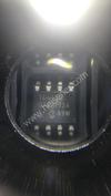
| Part Number | MM74HC4052M |
|---|---|
| Manufacturer | Fairchild/ON Semiconductor |
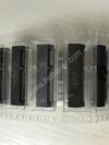
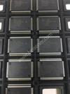
| Description | IC MUX/DEMUX DUAL 4X1 16SOIC |
| Datasheet | |
| Package | 16-SOIC (0.154", 3.90mm Width) |
| ECAD |
|
| In Stock | 16,056 piece(s) |
| Unit Price | Request a Quote |
| Lead Time | Can Ship Immediately |
| Estimated Delivery Time | Apr 29 - May 4 (Choose Expedited Shipping) |
| Request for Quotation |
|
| Payment Methods | |
| Delivery Services |
Part Number # MM74HC4052M (Interface - Analog Switches, Multiplexers, Demultiplexers) is manufactured by Fairchild/ON Semiconductor and distributed by Heisener. Being one of the leading electronics distributors, we carry many kinds of electronic components from some of the world’s top class manufacturers. Their quality is guaranteed by its stringent quality control to meet all required standards.
For MM74HC4052M specifications/configurations, quotation, lead time, payment terms of further enquiries please have no hesitation to contact us. To process your RFQ, please add MM74HC4052M with quantity into BOM. Heisener.com does NOT require any registration to request a quote of MM74HC4052M.
| Manufacturer | Fairchild/ON Semiconductor |
| Category | Integrated Circuits (ICs) - Interface - Analog Switches, Multiplexers, Demultiplexers |
| Package | 16-SOIC (0.154", 3.90mm Width) |
| ECAD |
|
| Series | - |
| Switch Circuit | SP4T |
| Multiplexer/Demultiplexer Circuit | 4:1 |
| Number of Circuits | 2 |
| On-State Resistance (Max) | 100 Ohm |
| Channel-to-Channel Matching (ΔRon) | 15 Ohm |
| Voltage - Supply, Single (V+) | 2 V ~ 6 V |
| Voltage - Supply, Dual (V±) | ±2 V ~ 6 V |
| Switch Time (Ton, Toff) (Max) | 41ns, 32ns |
| -3db Bandwidth | 35MHz |
| Charge Injection | - |
| Channel Capacitance (CS(off), CD(off)) | 5pF, 45pF |
| Current - Leakage (IS(off)) (Max) | 100nA |
| Crosstalk | -50dB @ 1MHz |
| Operating Temperature | -40°C ~ 85°C (TA) |
| Package / Case | 16-SOIC (0.154", 3.90mm Width) |
| Supplier Device Package | 16-SOIC |
Uri*****Lang
March 23, 2023
Alay*****ummers
March 22, 2023
Ald*****ugh
March 12, 2023


|
1808Y5000181GCR | Knowles Syfer, CAP CER 180PF 500V C0G/NP0 1808, 1808 (4520 Metric), - | View |

|
MP6400DJ-15-LF-P | Monolithic Power Systems Inc., IC SUPERVISORY PWM, SOT-23-6 Thin, TSOT-23-6, - | View |
|
|
ATTINY441-MMH | Microchip Technology, IC MCU 8BIT 4KB FLASH 20VQFN, 20-VFQFN Exposed Pad, - | View |

|
DF70844AD80FPV | Renesas Electronics America, IC MCU 32BIT 256KB FLASH 112LQFP, 112-LQFP, - | View |

|
ADS8471IRGZR | Texas Instruments, IC ADC 16BIT PAR 1M 48VQFN, 48-VFQFN Exposed Pad, - | View |
|
|
RWR89N1471FRS73 | Vishay Dale, RES 1.47K OHM 3W 1% WW AXIAL, Axial, - | View |
|
|
RLR20C3302GRRE6 | Vishay Dale, RES 33K OHM 2% 1/2W AXIAL, Axial, - | View |

|
MCR10EZPF56R0 | Rohm Semiconductor, RES SMD 56 OHM 1% 1/8W 0805, 0805 (2012 Metric), - | View |

|
ERA-1ARW1131C | Panasonic Electronic Components, RES SMD 1.13K OHM 1/20W 0201, 0201 (0603 Metric), - | View |

|
311-43-145-41-001000 | Mill-Max Manufacturing Corp., CONN SKT STRIP 45PIN .100 LNG TL, -, - | View |
|
|
DW-28-19-F-S-1005 | Samtec Inc., .025" BOARD SPACERS, -, - | View |
|
|
L777SDC37PA4CH3R | Amphenol Commercial Products, CONN D-SUB PLUG 37POS R/A SOLDER, -, - | View |

We guarantee 100% customer satisfaction.
Our experienced sales team and tech support team back our services to satisfy all our customers.

We provide 90 days warranty.
If the items you received were not in perfect quality, we would be responsible for your refund or replacement, but the items must be returned in their original condition.
| Part Number | Manufacturer | Description | Stock |
MM74HC4052M |
Fairchild Semiconductor Corporation | 44 |
| Part Number | Manufacturer | Description | Stock |
MM74HC4052M |
Fairchild Semiconductor Corporation |
Analog Multiplexer Dual 4:1 16-Pin TSSOP T/R |
13550 |
MM74HC4052MTC |
Fairchild Semiconductor Corporation |
Analog Multiplexer Dual 4:1 16-Pin TSSOP T/R |
13550 |
MM74HC4052MTCX |
Fairchild Semiconductor Corporation |
Analog Multiplexer Dual 4:1 16-Pin TSSOP T/R |
13550 |
MM74HC4052MX |
Fairchild Semiconductor Corporation |
IC MUX/DEMUX DUAL 4X1 16SOIC |
0 |
| Part Number | Manufacturer | Description | Stock |
MM74HC4052MTC D# MM74HC4052MTC-ND |
ON Semiconductor |
IC MUX/DEMUX DUAL 4X1 16TSSOP |
0 |
MM74HC4052MTCX D# MM74HC4052MTCX-ND |
ON Semiconductor |
IC MUX/DEMUX DUAL 4X1 16TSSOP |
0 |
MM74HC4052M D# MM74HC4052M-ND |
ON Semiconductor |
IC MUX/DEMUX DUAL 4X1 16SOIC |
0 |
MM74HC4052MX D# MM74HC4052MXTR-ND |
ON Semiconductor |
IC MUX/DEMUX DUAL 4X1 16SOIC |
0 |
| Part Number | Manufacturer | Description | Stock |
MM74HC4052M D# MM74HC4052M |
Fairchild Semiconductor Corporation |
Industry Leading ISO:9001/AS9120A Stocking Distributor of Obsolete & Hard to Find IC's/Semi's, Specializing in Altera/Xilinx. In-House Counterfeit Detection Lab. In Business 20 Years. Free Shipping on Orders Over $250. Buy American, Buy Direct |
66 |
| Part Number | Manufacturer | Description | Stock |
MM74HC4052M |
Fairchild Semiconductor Corporation |
In stock shipping within 2days |
251 |
MM74HC4052MX |
Fairchild Semiconductor Corporation |
In stock shipping within 2days |
1334 |
MM74HC4052MTCX |
Fairchild Semiconductor Corporation |
In stock shipping within 2days |
2630 |
| Part Number | Manufacturer | Description | Stock |
MM74HC4052MX |
Fairchild Semiconductor Corporation |
Stock |
160 |
| Part Number | Manufacturer | Description | Stock |
MM74HC4052MX |
Fairchild Semiconductor Corporation |
OEM/CM QUOTES ONLY | NO BROKERS |
43500 |
MM74HC4052MTC |
FAIR |
OEM/CM QUOTES ONLY | NO BROKERS |
2900 |
MM74HC4052MXNL |
Fairchild Semiconductor Corporation |
OEM/CM QUOTES ONLY | NO BROKERS |
4826 |
MM74HC4052M |
N |
OEM/CM QUOTES ONLY | NO BROKERS |
5800 |
74HC4052MXMM74HC4052MX |
Fairchild Semiconductor Corporation |
OEM/CM QUOTES ONLY | NO BROKERS |
2000 |
MM74HC4052MTCX |
OEM/CM QUOTES ONLY | NO BROKERS |
3712 |
| Part Number | Manufacturer | Description | Stock |
MM74HC4052M |
Fairchild Semiconductor Corporation |
In stock |
17 |
| Part Number | Manufacturer | Description | Stock |
MM74HC4052MTCX |
Fairchild Semiconductor Corporation |
OEM/CM Immediate delivery |
2630 |
MM74HC4052MX |
Fairchild Semiconductor Corporation |
OEM/CM Immediate delivery |
2470 |
MM74HC4052M |
Fairchild Semiconductor Corporation |
OEM/CM Immediate delivery |
151 |
| Part Number | Manufacturer | Description | Stock |
MM74HC4052MTCX D# NS-MM74HC4052MTCX |
Fairchild Semiconductor Corporation |
OEM/CM ONLY |
1653 |
MM74HC4052MX D# NS-MM74HC4052MX |
Fairchild Semiconductor Corporation |
OEM/CM ONLY |
9942 |
| Part Number | Manufacturer | Description | Stock |
MM74HC4052MX |
National Semiconductor Corporation |
Analog Multiplexer, Single, 4 Channel, 16 Pin, Plastic, SOP |
388 |
MM74HC4052M |
Fairchild Semiconductor Corporation |
Analog Multiplexer, Single, 4 Channel, 16 Pin, Plastic, SOP |
5 |
| Part Number | Manufacturer | Description | Stock |
MM74HC4052MX D# MM74HC4052MX |
Fairchild Semiconductor Corporation |
Semiconductor |
89 |
| Part Number | Manufacturer | Description | Stock |
MM74HC4052MX |
Fairchild Semiconductor Corporation |
OEM/CM ONLY |
37516 |
MM74HC4052MTCX |
Fairchild Semiconductor Corporation |
OEM/CM ONLY |
2042 |
MM74HC4052M |
Fairchild Semiconductor Corporation |
OEM/CM ONLY |
13626 |
MM74HC4052MTC |
Fairchild Semiconductor Corporation |
OEM/CM ONLY |
2516 |
74HC4052MXMM74HC4052MX |
Fairchild Semiconductor Corporation |
OEM/CM ONLY |
1755 |
MM74HC4052MXNL |
Fairchild Semiconductor Corporation |
OEM/CM ONLY |
4176 |
| Part Number | Manufacturer | Description | Stock |
MM74HC4052M |
Fairchild Semiconductor Corporation |
IN stock Immediate delivery |
146 |
MM74HC4052MTCX |
Fairchild Semiconductor Corporation |
IN stock Immediate delivery |
2645 |
MM74HC4052MX |
FARCHILD |
IN stock Immediate delivery |
2485 |
| Part Number | Manufacturer | Description | Stock |
MM74HC4052MTCX |
Fairchild Semiconductor Corporation |
shipping today |
17 |
MM74HC4052MX |
Fairchild Semiconductor Corporation |
shipping today |
231 |
| Part Number | Manufacturer | Description | Stock |
MM74HC4052MX |
mfr |
RFQ |
770 |
MM74HC4052MXCT |
Fairchild Semiconductor Corporation |
RFQ |
10293 |
MM74HC4052M |
mfr |
RFQ |
13049 |
MM74HC4052MXTR |
Fairchild Semiconductor Corporation |
RFQ |
14645 |
| Part Number | Manufacturer | Description | Stock |
MM74HC4052M D# 1013866 |
ON Semiconductor |
RoHS: Compliant
Min Qty: 1
Container: Each
|
0 |
Heisener's commitment to quality has shaped our processes for sourcing, testing, shipping, and every step in between. This foundation underlies each component we sell.

Do you have any question about MM74HC4052M?
+86-755-83210559 ext. 813


Scan to view this page