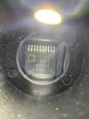
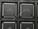
Part Number # MPC8306SVMADDCA (Embedded - Microprocessors) is manufactured by NXP and distributed by Heisener. Being one of the leading electronics distributors, we carry many kinds of electronic components from some of the world’s top class manufacturers. Their quality is guaranteed by its stringent quality control to meet all required standards.
For MPC8306SVMADDCA specifications/configurations, quotation, lead time, payment terms of further enquiries please have no hesitation to contact us. To process your RFQ, please add MPC8306SVMADDCA with quantity into BOM. Heisener.com does NOT require any registration to request a quote of MPC8306SVMADDCA.
Received Quickly. Excellent Communication. Capacitors Look Excellent.
Ashto*****ierrez
April 6, 2023
★★★★★
These are the most popular variety of components of different types!
Nehem*****ommen
April 4, 2023
★★★★★
Worked like it was intended.
Jav*****Leon
March 24, 2023
★★★★★
You guys and girls are fantastic! The selection is fantastic and service is great.
Mcken*****ayton
March 24, 2023
★★★★★
Great dealing with you Guys. Thanks for a very prompt delivery.
Anth*****Gopal
March 11, 2023
★★★★★
I have always get a fast response from Heisener with my orders. As a small business owner I greatly appreciate that I can order as little as 1 item as opposed to other companies who require you place a larger minimum order.
Emmaly*****taneda
March 9, 2023
★★★★★
Very effective shopping path, service steady as a rock, keep up the great work.
Bai***** Ray
February 27, 2023
★★★★★
quick delivery, received with well packaged, exactly as listed - Thanks
Write a Review
Thanks for Your Review!
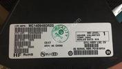
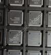
MPC8306SVMADDCA Packaging
MPC8306SVMADDCA FAQ
1. How to order MPC8306SVMADDCA on Heisener?
Currently, Heisener only provide peer-to-peer order processing. While you submit the RFQ, our professional agent will contact you with the competitive prices in the global market, and our agent will prompt you to finish the order if you accept our offers.
2. How does Heisener guarantee that MPC8306SVMADDCA is from the original manufacturer or authorized agents?
We have a professional and experienced quality control team to strictly verify and test the MPC8306SVMADDCA.
All suppliers must pass our qualification reviews before they can publish their products including MPC8306SVMADDCA on Heisener; we pay more attention to the channels and quality of MPC8306SVMADDCA products than any other customer.
We strictly implement supplier audits, so you can purchase with confidence.
3. Are the MPC8306SVMADDCA price and inventory displayed accurate?
The price and inventory of MPC8306SVMADDCA fluctuates frequently and cannot be updated in time, it will be updated periodically within 24 hours. And, our quotation usually expires after 5 days.
4. What forms of payment are accepted?
Wire Transfer, PayPal, Alipay, Wechat, Credit Card, Western Union, MoneyGram, and Escrow are all acceptable.
Warm Tips: Some orders in certain payment forms may require handling fee.
5. How is the shipping arranged?
Customers can choose industry-leading freight companies, including DHL, UPS, FedEx, TNT, and Registered Mail. Shipping insurance is also available.
Once your order has been processed for shipment, our salesperson will send you an email advising you of the shipping status and tracking number.
Warm Tips: It may take up to 24 hours for the carriers to display tracking information. Usually, express delivery takes 3-5 days, and registered mail takes 25-60 days.
6. What is the process for return or replacement of MPC8306SVMADDCA?
All goods will implement Pre-Shipment Inspection (PSI), selected at random from all batches of your order to do a systematic inspection before arranging the shipment.
If there is something wrong with the MPC8306SVMADDCA we delivered, we will accept the replacement or return of the MPC8306SVMADDCA only when all of the below conditions are fulfilled:
(1)Such as a deficiency in quantity, delivery of wrong items, and apparent external defects (breakage and rust, etc.), and we acknowledge such problems.
(2)We are informed of the defect described above within 90 days after the delivery of MPC8306SVMADDCA.
(3)The PartNo is unused and only in the original unpacked packaging.
Two processes to return the products:
(1)Inform us within 90 days
(2)Obtain Requesting Return Authorizations
7.How to contact us to get technical supports, such as MPC8306SVMADDCA pin diagram, MPC8306SVMADDCA datasheet?
If you need any after-sales service, please do not hesitate to contact us.
Our experienced sales team and tech support team back our services to satisfy all our customers.
Quality Guarantees
We provide 90 days warranty.
If the items you received were not in perfect quality, we would be responsible for your refund or replacement, but the items must be returned in their original condition.
Global Supply Chains - Reliable and Authorized Distributor Resources
Part Number
Manufacturer
Description
Stock
MPC8306SVMADDCA
D# V36:1790_07199288
NXP Semiconductors
MPU PowerQUICC II Pro MPC83xx Processor RISC 32bit 0.09um 266MHz 1.8V/3.3V 369-Pin MAP-BGA Tray
RoHS: Compliant
0
Part Number
Manufacturer
Description
Stock
MPC8306SVMADDCA
D# MPC8306SVMADDCA
NXP Semiconductors
MPU PowerQUICC II Pro RISC 32-Bit 266MHz 1.8V 369-Pin MAPBGA Brick - Bulk (Alt: MPC8306SVMADDCA)
RoHS: Compliant
0
Part Number
Manufacturer
Description
Stock
MPC8306SVMADDCA
D# MPC8306SVMADDCA
NXP Semiconductors
MPU PowerQUICC II Pro RISC 32-Bit 266MHz 1.8V 369-Pin MAPBGA Brick (Alt: MPC8306SVMADDCA)
0
Part Number
Manufacturer
Description
Stock
MPC8306SVMADDCA
Freescale Semiconductor
MPU, 32BIT, 266MHZ, MAPBGA-369
84
Part Number
Manufacturer
Description
Stock
MPC8306SVMADDCA
D# 2156-MPC8306SVMADDCA-ND
Rochester Electronics LLC
POWERQUICC POWER ARCH SOC, 266MH
671
Part Number
Manufacturer
Description
Stock
MPC8306SVMADDCA
NXP Semiconductors
RoHS: Compliant
pbFree: Yes
0
Part Number
Manufacturer
Description
Stock
MPC8306SVMADDCA
Freescale Semiconductor
OEM/CM QUOTES ONLY | NO BROKERS
2639
Part Number
Manufacturer
Description
Stock
MPC8306SVMADDCA
NXP Semiconductors
OEM/CM ONLY
109
Part Number
Manufacturer
Description
Stock
MPC8306SVMADDCA
Freescale Semiconductor
OEM/CM Immediate delivery
77
Part Number
Manufacturer
Description
Stock
MPC8306SVMADDCA
D# 13T4361
NXP Semiconductors
32 BIT MICROPROCESSOR-MPU, 266MHz, 369-MAPBGA, Product Range:PowerQUICC Family PowerQUICC II Pro Series Microprocessors, MPU Core Size:32bit, Program Memory Size:32KB, No. of Pins:369Pins, MPU Case Style:MAPBGA, CPU Speed:266MHz RoHS Compliant: Yes
RoHS: Compliant
Min Qty: 420
Container: Bulk
0
Part Number
Manufacturer
Description
Stock
MPC8306SVMADDCA
D# NS-MPC8306SVMADDCA
Freescale Semiconductor
OEM/CM ONLY
3321
Part Number
Manufacturer
Description
Stock
MPC8306SVMADDCA
Freescale Semiconductor
PowerQUICC Power Arch SoC, 266MHz, DDR2, HDLC, TDM, Enet, USB, 0 to 105C, Rev 1.1
RoHS: Compliant
671
Part Number
Manufacturer
Description
Stock
MPC8306SVMADDCA
Freescale Semiconductor
IN stock Immediate delivery
72
Part Number
Manufacturer
Description
Stock
MPC8306SVMADDCA
Freescale Semiconductor
shipping today
76
Part Number
Manufacturer
Description
Stock
MPC8306SVMADDCA
D# 25968018
NXP Semiconductors
MPU PowerQUICC II Pro MPC83xx Processor RISC 32bit 0.09um 266MHz 1.8V/3.3V 369-Pin MAP-BGA Tray
RoHS: Compliant
0
Part Number
Manufacturer
Description
Stock
MPC8306SVMADDCA
Freescale Semiconductor
RFQ
7753
Certified Quality
Heisener's commitment to quality has shaped our processes for sourcing, testing, shipping, and every step in between. This foundation underlies each component we sell.