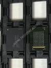
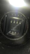
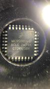
Part Number | R5F1076CGSP#X0 |
---|---|
Manufacturer | Renesas Electronics America |
Description | IC MCU 16BIT 32KB FLASH 20LSSOP |
Datasheet | R5F1076CGSP#X0 Datasheet |
Package | 20-LSSOP (0.173", 4.40mm Width) |
In Stock | 456 piece(s) |
Unit Price | $ 1.8354 * |
Lead Time | To be Confirmed |
Estimated Delivery Time | Jan 21 - Jan 26 (Choose Expedited Shipping) |
Request for Quotation |
|
Part Number # R5F1076CGSP#X0 (Embedded - Microcontrollers) is manufactured by Renesas Electronics America and distributed by Heisener. Being one of the leading electronics distributors, we carry many kinds of electronic components from some of the world’s top class manufacturers. Their quality is guaranteed by its stringent quality control to meet all required standards.
For R5F1076CGSP#X0 specifications/configurations, quotation, lead time, payment terms of further enquiries please have no hesitation to contact us. To process your RFQ, please add R5F1076CGSP#X0 with quantity into BOM. Heisener.com does NOT require any registration to request a quote of R5F1076CGSP#X0.
Manufacturer | Renesas Electronics America |
Category | Integrated Circuits (ICs) - Embedded - Microcontrollers |
Datasheet | R5F1076CGSP#X0Datasheet |
Package | 20-LSSOP (0.173", 4.40mm Width) |
Series | RL78/I1A |
Core Processor | RL78 |
Core Size | 16-Bit |
Speed | 32MHz |
Connectivity | I2C, LIN, UART/USART |
Peripherals | DMA, LVD, POR, PWM, WDT |
Number of I/O | 13 |
Program Memory Size | 32KB (32K x 8) |
Program Memory Type | FLASH |
EEPROM Size | - |
RAM Size | 2K x 8 |
Voltage - Supply (Vcc/Vdd) | 2.7 V ~ 5.5 V |
Data Converters | A/D 6x8/10b |
Oscillator Type | Internal |
Operating Temperature | -40°C ~ 105°C (TA) |
Mounting Type | - |
Package / Case | 20-LSSOP (0.173", 4.40mm Width) |
Supplier Device Package | 20-LSSOP |
Datasheet
RL78/I1A
RENESAS MCU
True Low Power Platform, High Resolution PWM and Rich Analog, 2.7 V to 5.5 V operation, 32 to 64 Kbyte Flash,
for Inverter Control, Digital Power Control and Lighting Control Applications
Page 1 of 105
R01DS0171EJ0320
Rev.3.20
Sep 29, 2017
R01DS0171EJ0320 Rev.3.20
Sep 29, 2017
1. OUTLINE
1.1 Features
Ultra-Low Power Technology
2.7 V to 5.5 V operation from a single supply
Stop (RAM retained): 0.23 µA, (LVD enabled): 0.31 µA
Halt (RTC + LVD): 0.60 µA
Operating: 156.25 µA/MHz
16-bit RL78 CPU Core
Delivers 41 DMIPS at maximum operating frequency of
32 MHz
Instruction execution: 86% of instructions can be
executed in 1 to 2 clock cycles
CISC architecture (Harvard) with 3-stage pipeline
Multiply signed & unsigned: 16 x 16 to 32-bit result in 1
clock cycle
MAC: 16 x 16 to 32-bit result in 2 clock cycles
16-bit barrel shifter for shift & rotate in 1 clock cycle
1-wire on-chip debug function
Main Flash Memory
Density: 32 KB to 64 KB
Block size: 1 KB
On-chip single voltage flash memory with protection from
block erase/writing
Self-programming with secure boot swap function and
flash shield window function
Data Flash Memory
Data flash with background operation
Data flash size: 4 KB
Erase cycles: 1 million (typ.)
Erase/programming voltage: 2.7 V to 5.5 V
RAM
2 KB to 4 KB size options
Supports operands or instructions
Back-up retention in all modes
High-speed On-chip Oscillator
32 MHz with +/ 1% accuracy over voltage (2.7 V to 5.5
V) and temperature (20°C to 85°C)
Pre-configured settings: 32 MHz, 24 MHz, 16 MHz, 12
MHz, 8 MHz, 6 MHz, 4 MHz, 3 MHz, 2 MHz & 1 MHz
Reset and Supply Management
Power-on reset (POR) monitor/generator
Low voltage detection (LVD) with 6 setting options
(Interrupt and/or reset function)
Data Memory Access (DMA) Controller
Up to 2 fully programmable channels
Transfer unit: 8- or 16-bit
16-bit timers KB0 to KB2, and KC0 for PWM output
16-bit timers KB0 to KB2: maximum 6 outputs (3 channels 2)
Smooth start function, dithering function, forced output
stop function (unsynchronized with comparator or external
interrupt) enables over-voltage protection, over-current
protection and peak current control, and single/interleave
PFC function
Average resolution < 0.98 nsec output, 64 MHz (when
using PLL) + dithering option
16-bit timer KC0 (1 channel × 6 (output))
PWM output gating function by interlocking with 16-bit
timers KB0, KB1, and KB2
Extended-Function Timers
Multi-function 16-bit timers: Up to 8 channels
Real-time clock (RTC): 1 channel (full calendar and
alarm function with watch correction function)
Interval timer: 12-bit, 1 channel
15 kHz watchdog timer: 1 channel (window function)
Multiple Communication Interfaces
Up to 1 channel x I2C multi-master (SMBus/PMBus
support)
Up to 1 channel x CSI/SPI (7-, 8-bit)
Up to 3 channels x UART (7-, 8-, 9-bit),
DALI support 1 channel (8-, 16-, 17-, 24-bit, master and
slave)
Up to 1 channel x LIN
Rich Analog
ADC: Up to 11 channels, 8/10-bit resolution, 2.125 µs
conversion time
Supports 2.7 V
Internal voltage reference (1.45 V)
Comparator: High response time 70 ns (typ.), up to 6
channels, internal DAC 3 channels 8-bit resolution,
window comparator mode
PGA (x4 to x32): 6 input channels
On-chip temperature sensor
Safety Features (IEC or UL 60730 compliance)
Flash memory CRC calculation
RAM parity error check
RAM/SFR write protection
Illegal memory access detection
Clock stop/frequency detection
ADC self-test
General Purpose I/O
5-V tolerant, high-current (up to 8.5 mA per pin)
Open-drain, internal pull-up support
Operating Ambient Temperature
Standard: 40°C to +105°C
Extend: 40°C to +125°C
Package Type and Pin Count
SSOP: 20, 30, 38
RL78/I1A 1. OUTLINE Page 2 of 105R01DS0171EJ0320 Rev.3.20 Sep 29, 2017 ○ ROM, RAM capacities Flash ROM Data flash RAM RL78/I1A 20 pins 30 pins 38 pins 64 KB 4 KB 4 KB Note R5F107AE R5F107DE 32 KB 4 KB 2 KB R5F1076C R5F107AC Note This is about 3 KB when the self-programming function and data flash function are used.
RL78/I1A 1. OUTLINE Page 3 of 105R01DS0171EJ0320 Rev.3.20 Sep 29, 2017 1.2 List of Part Numbers Figure 1-1. Part Number, Memory Size, and Package of RL78/I1A Part No. R 5 F 1 0 7 D E G x x x S P # V 0 Package type: ROM number (Omitted with blank products) ROM capacity: RL78/I1A group Renesas MCU Renesas semiconductor product SP: LSSOP, 0.65 mm pitch SSOP, 0.65 mm pitch C: 32 KB E: 64 KB Pin count: 6: 20-pin A: 30-pin D: 38-pin Classification: G: Operating ambient temperature: −40°C to 105°C M: Operating ambient temperature: −40°C to 125°C Memory type: F: Flash memory Package specification: #V0: Tray (LSSOP30, SSOP38), Tube (LSSOP20) #X0: Embossed tape (LSSOP, SSOP) Pin count Package Operating Ambient Temperature Part Number 20 pins 20-pin plastic LSSOP (4.4 6.5) TA = 40 to +105C R5F1076CGSP#V0, R5F1076CGSP#X0 TA = 40 to +125C R5F1076CMSP#V0, R5F1076CMSP#X0 30 pins 30-pin plastic LSSOP (7.62 mm (300)) TA = 40 to +105C R5F107ACGSP#V0, R5F107AEGSP#V0, R5F107ACGSP#X0, R5F107AEGSP#X0 TA = 40 to +125C R5F107ACMSP#V0, R5F107AEMSP#V0, R5F107ACMSP#X0, R5F107AEMSP#X0 38 pins 38-pin plastic SSOP (7.62 mm (300)) TA = 40 to +105C R5F107DEGSP#V0, R5F107DEGSP#X0 TA = 40 to +125C R5F107DEMSP#V0, R5F107DEMSP#X0 Caution The ordering part numbers represent the numbers at the time of publication. For the latest ordering part numbers, refer to the target product page of the Renesas Electronics website.
RL78/I1A 1. OUTLINE Page 4 of 105R01DS0171EJ0320 Rev.3.20 Sep 29, 2017 1.3 Pin Configuration (Top View) 1.3.1 20-pin products 20-pin plastic LSSOP (4.4 x 6.5) 20 19 18 17 16 15 14 13 12 11 1 2 3 4 5 6 7 8 9 10 P22/ANI2/CMP0P P24/ANI4/CMP1P P25/ANI5/CMP2P P147/CMPCOM/ANI18/(CMP3P) P10/TxD0/TKCO00/INTP20/SCLA0/(DALITxD4) P11/RxD0/TKCO01/INTP21/SDAA0/(TI07)/(DALIRxD4)/(TxRx4)/(INTP0) P200/TKBO00/INTP22 P201/TKBO01 P202/TKBO10/(INTP21) P203/TKBO11/TKCO02/(INTP20) P21/ANI1/AVREFM P20/ANI0/AVREFP P40/TOOL0 RESET P137/INTP0 P122/X2/EXCLK P121/X1 REGC VSS VDD Caution Connect the REGC pin to Vss via a capacitor (0.47 to 1 F). Remarks 1. For pin identification, see 1.4 Pin Identification. 2. Functions in parentheses in the above figure can be assigned via settings in the peripheral I/O redirection register (PIOR1) or the input switch control register (ISC). See Figure 4-8 Format of Peripheral I/O Redirection Register (PIOR1) and Figure 15-20 Format of Input Switch Control Register (ISC) in the RL78/I1A User's Manual. 3. The shared function CMP3P can be assigned to P147 by setting the CMPSEL0 bit in the comparator input switch control register (CMPSEL).
RL78/I1A 1. OUTLINE Page 5 of 105R01DS0171EJ0320 Rev.3.20 Sep 29, 2017 1.3.2 30-pin products 30-pin plastic LSSOP (7.62 mm (300)) 30 29 28 27 26 25 24 23 22 21 20 19 18 17 16 1 2 3 4 5 6 7 8 9 10 11 12 13 14 15 P21/ANI1/AVREFM P22/ANI2/CMP0P P24/ANI4/CMP1P P25/ANI5/CMP2P P26/ANI6/CMP3P P27/ANI7/CMP4P P147/CMPCOM/ANI18 P10/TxD0/TKCO00/INTP20/SCLA0/(DALITxD4) P11/RxD0/TKCO01/INTP21/SDAA0/(TI07)/(DALIRxD4)/(TxRx4)/(INTP0) P200/TKBO00/INTP22 P201/TKBO01 P202/TKBO10/(INTP21) P203/TKBO11/TKCO02/(INTP20) P204/TKBO20/TKCO03 P205/TKBO21/TKCO04/DALITxD4 P20/ANI0/AVREFP P03/RxD1/CMP5P/ANI16 P02/TxD1/ANI17 P120/ANI19 P40/TOOL0 RESET P137/INTP0 P122/X2/EXCLK P121/X1 REGC VSS VDD P31/TI03/TO03/INTP4 P77/INTP11 P206/TKCO05/DALIRxD4/TxRx4/INTP23 Caution Connect the REGC pin to Vss via a capacitor (0.47 to 1 F). Remarks 1. For pin identification, see 1.4 Pin Identification. 2. Functions in parentheses in the above figure can be assigned via settings in the peripheral I/O redirection register (PIOR1) or the input switch control register (ISC). See Figure 4-8 Format of Peripheral I/O Redirection Register (PIOR1) and Figure 15-20 Format of Input Switch Control Register (ISC) in the RL78/I1A User's Manual.
RL78/I1A 1. OUTLINE Page 6 of 105R01DS0171EJ0320 Rev.3.20 Sep 29, 2017 1.3.3 38-pin products 38-pin plastic SSOP (7.62 mm (300)) 38 37 36 35 34 33 32 31 30 29 28 27 26 25 24 23 22 21 20 1 2 3 4 5 6 7 8 9 10 11 12 13 14 15 16 17 18 19 P20/ANI0/AVREFP P03/RxD1/CMP5P/ANI16 P02/TxD1/ANI17 P120/ANI19 P40/TOOL0 RESET P124/XT2/EXCLKS P123/XT1 P137/INTP0 P122/X2/EXCLK P121/X1 REGC VSS VDD P31/TI03/TO03/INTP4 P77/INTP11 P76/INTP10 P75/INTP9 P06/TI06/TO06 P21/ANI1/AVREFM P22/ANI2/CMP0P P24/ANI4/CMP1P P25/ANI5/CMP2P P26/ANI6/CMP3P P27/ANI7/CMP4P P147/CMPCOM/ANI18 P10/SO00/TxD0/TKCO00/INTP20/SCLA0/(DALITxD4) P11/SI00/RxD0/TKCO01/INTP21/SDAA0/(TI07)/(DALIRxD4)/(TxRx4)/(INTP0) P12/SCK00/(TKCO03) P200/TKBO00/INTP22 P201/TKBO01 P202/TKBO10/(INTP21) P203/TKBO11/TKCO02/(INTP20) P204/TKBO20/TKCO03 P205/TKBO21/TKCO04/DALITxD4 P206/TKCO05/DALIRxD4/TXRx4/INTP23 P30/INTP3/RTC1HZ P05/TI05/TO05 Caution Connect the REGC pin to Vss via a capacitor (0.47 to 1 F). Remarks 1. For pin identification, see 1.4 Pin Identification. 2. Functions in parentheses in the above figure can be assigned via settings in the peripheral I/O redirection register (PIOR1) or the input switch control register (ISC). See Figure 4-8 Format of Peripheral I/O Redirection Register (PIOR1) and Figure 15-20 Format of Input Switch Control Register (ISC) in the RL78/I1A User's Manual.
RL78/I1A 1. OUTLINE Page 7 of 105R01DS0171EJ0320 Rev.3.20 Sep 29, 2017 1.4 Pin Identification ANI0 to ANI2, ANI4 to ANI7, ANI16 to ANI19: Analog Input AVREFM: Analog Reference Voltage Minus AVREFP: Analog Reference Voltage Plus CMP0P to CMP5P: Comparator Analog Input CMPCOM: Comparator External Reference Voltage EXCLK: External Clock Input (Main System Clock) EXCLKS: External Clock Input (Subsystem Clock) INTP0, INTP3, INTP4, INTP9, INTP10, INTP11, INTP20 to INTP23: Interrupt Request from Peripheral P02, P03, P05, P06: Port 0 P10 to P12: Port 1 P20 to P22, P24 to P27: Port 2 P30, P31: Port 3 P40: Port 4 P75 to P77: Port 7 P120 to P124: Port 12 P137: Port 13 P147: Port 14 P200 to P206: Port 20 REGC: Regulator Capacitance RESET: Reset RTC1HZ: Real-time Clock Correction Clock (1 Hz) Output RxD0, RxD1, DALIRxD4: Receive Data SCK00: Serial Clock Input/Output SCLA0: Serial Clock Input/Output SDAA0: Serial Data Input/Output SI00: Serial Data Input SO00: Serial Data Output TI03, TI05, TI06, TI07: Timer Input TO03, TO05, TO06, TKBO00, TKBO01 to TKBO20, TKBO21, TKCO00 to TKCO05: Timer Output TOOL0: Data Input/Output for Tool TxRx4: Serial Data Input/Output for Single Wired UART TxD0, TxD1 DALITxD4: Transmit Data VDD: Power Supply VSS: Ground X1, X2: Crystal Oscillator (Main System Clock) XT1, XT2: Crystal Oscillator (Subsystem Clock)
RL78/I1A 1. OUTLINE Page 8 of 105R01DS0171EJ0320 Rev.3.20 Sep 29, 2017 1.5 Block Diagram 1.5.1 20-pin products PORT 1 P10, P11 PORT 2 P20 to P22, P24, P25 5 PORT 4 2 PORT 12 P121, P122 P40 VOLTAGE REGULATOR REGC INTERRUPT CONTROL RAM DATA FLASH MEMORY POWER ON RESET/ VOLTAGE DETECTOR POR/LVD CONTROL RESET CONTROL SYSTEM CONTROL RESET X1/P121 X2/EXCLK/P122 HIGH-SPEED ON-CHIP OSCILLATOR ON-CHIP DEBUG TOOL0/P40 SERIAL ARRAY UNIT0 (4ch) UART0 RxD0/P11 TxD0/P10 TIMER ARRAY UNIT (8ch) ch2 ch3 ch0 ch1 ch4 ch5 ch6 ch7 INTP0/P137 RxD0/P11 A/D CONVERTER 5 3 4 ANI0/P20 to ANI2/P22, ANI4/P24, ANI5/P25 CMP0P/P22, CMP1P/P24, CMP2P/P25, (CMP3P/P147) AVREFP/P20 CMPCOM/P147 AVREFM/P21 2 PORT 13 P137 (TI07)/RxD0/P11(LIN-bus, DMX512) BCD ADJUSTMENT VSSVDD SERIAL INTERFACE IICA SDAA0/P11 SCLA0/P10 INTP22/P200 INTP20/P10(INTP20/P203) INTP21/P11(INTP21/P202) MULTIPLIER& DIVIDER, MULTIPLY- ACCUMULATOR PROGRAMMABLE GAIN AMPLIFIER 3 CMP0P/P22, CMP1P/P24, CMP2P/P25, (CMP3P/P147) COMPARATOR 3 16-bit TIMER KB0, KB1 16-bit TIMER KC0 ANI18/P147 SERIAL ARRAY UNIT4 (2ch) UART4 DALI, DMX512 SINGLE-WIRE UART LIN-bus, DMX512 (DALIRxD4/P11) (DALITxD4/P10) (TxRx4/P11) DIRECT MEMORY ACCESS CONTROL PORT 20 P200 to P2034 PORT 14 P147 TKBO00/P200, TKBO01/P201, TKBO10/P202, TKBO11/P203 TKCO00/P10, TKCO01/P11, TKCO02/P203 RL78 CPU CORE CODE FLASH MEMORY DATA FLASH MEMORY LOW-SPEED ON-CHIP OSCILLATOR 12- BIT INTERVAL TIMER WINDOW WATCHDOG TIMER REAL-TIME CLOCK CRC Remarks 1. Functions in parentheses in the above figure can be assigned via settings in the peripheral I/O redirection register (PIOR1) or the input switch control register (ISC). See Figure 4-8 Format of Peripheral I/O Redirection Register (PIOR1) and Figure 15-20 Format of Input Switch Control Register (ISC) in the RL78/I1A User's Manual. 2. The shared function CMP3P can be assigned to P147 by setting the CMPSEL0 bit in the comparator input switch control register (CMPSEL).
RL78/I1A 1. OUTLINE Page 9 of 105R01DS0171EJ0320 Rev.3.20 Sep 29, 2017 1.5.2 30-pin products PORT 1 P10, P11 PORT 2 P20 to P22, P24 to P27 7 PORT 3 P31 PORT 4 2 PORT 12 P121, P122 P40 VOLTAGE REGULATOR REGC INTERRUPT CONTROL RAM DATA FLASH MEMORY POWER ON RESET/ VOLTAGE DETECTOR POR/LVD CONTROL RESET CONTROL SYSTEM CONTROL RESET X1/P121 X2/EXCLK/P122 HIGH-SPEED ON-CHIP OSCILLATOR ON-CHIP DEBUG TOOL0/P40 SERIAL ARRAY UNIT0 (4ch) UART0 UART1 RxD0/P11 TxD0/P10 RxD1/P03 TxD1/P02 TIMER ARRAY UNIT (8ch) ch2 ch3TI03/TO03/P31 ch0 ch1 ch4 ch5 ch6 ch7 INTP11/P77 INTP0/P137 INTP4/P31 RxD0/P11 A/D CONVERTER 76 6 ANI0/P20 to ANI2/P22, ANI4/P24 to ANI7/P27 CMP0P/P22, CMP1P/P24 to CMP4P/P27, CMP5P/P03 AVREFP/P20 CMPCOM/P147 AVREFM/P21 2 P120 PORT 13 P137 BCD ADJUSTMENT VSSVDD SERIAL INTERFACE IICA SDAA0/P11 SCLA0/P10 INTP22/P200 INTP23/P206 INTP20/P10(INTP20/P203) INTP21/P11(INTP21/P202) MULTIPLIER& DIVIDER, MULTIPLY- ACCUMULATOR PORT 0 P02, P032 PROGRAMMABLE GAIN AMPLIFIER 6 CMP0P/P22, CMP1P/P24 to CMP4P/P27, CMP5P/P03 COMPARATOR 6 16-bit TIMER KB0 to KB2 16-bit TIMER KC0 4 ANI16/P03, ANI17/P02, ANI18/P147, ANI19/P120 SERIAL ARRAY UNIT4 (2ch) UART4 SINGLE-WIRE UART DALIRxD4/P206(DALIRxD4/P11) DALITxD4/P205(DALITxD4/P10) TxRx4/P206(TXRX4/P11) DIRECT MEMORY ACCESS CONTROL PORT 7 P77 PORT 20 P200 to P2067 PORT 14 P147TKBO00/P200, TKBO01/P201, TKBO10/P202, TKBO11/P203, TKBO20/P204, TKBO21/P205 TKCO00/P10, TKCO01/P11, TKCO02/P203,TKCO03/P204, TKCO04/P205,TKCO05/P206 (TI07)/RxD0/P11(LIN-bus, DMX512) RL78 CPU CORE CODE FLASH MEMORY DATA FLASH MEMORY LIN-bus, DMX512 WINDOW WATCHDOG TIMER REAL-TIME CLOCK LOW-SPEED ON-CHIP OSCILLATOR 12- BIT INTERVAL TIMER CRC DALI, DMX512 Remark Functions in parentheses in the above figure can be assigned via settings in the peripheral I/O redirection register (PIOR1) or the input switch control register (ISC). See Figure 4-8 Format of Peripheral I/O Redirection Register (PIOR1) and Figure 15-20 Format of Input Switch Control Register (ISC) in the RL78/I1A User's Manual.
Daph*****rosby
December 19, 2020
Tuc***** Hora
December 18, 2020
Pao*****Ghose
December 17, 2020
Ezra*****gins
December 9, 2020
Syl***** Mand
December 3, 2020
Rhet*****averi
November 30, 2020
Mic*****Colon
November 29, 2020
Raina*****rabarti
November 23, 2020
We guarantee 100% customer satisfaction.
Our experienced sales team and tech support team back our services to satisfy all our customers.
We provide 90 days warranty.
If the items you received were not in perfect quality, we would be responsible for your refund or replacement, but the items must be returned in their original condition.
Payment Methods | |
Delivery Services |
Heisener's commitment to quality has shaped our processes for sourcing, testing, shipping, and every step in between. This foundation underlies each component we sell.