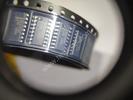
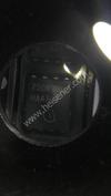
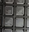
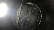
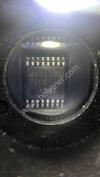
| Part Number | ISL54105ACRZ |
|---|---|
| Manufacturer | Renesas Electronics America |
| Description | IC TMDS REGENERATOR 72-QFN |
| Datasheet | |
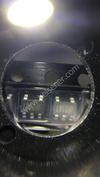
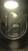
| Package | 72-VFQFN Exposed Pad |
| ECAD |
|
| In Stock | 24,000 piece(s) |
| Unit Price | $ 24.5583 * |
| Lead Time | Can Ship Immediately |
| Estimated Delivery Time | Apr 29 - May 4 (Choose Expedited Shipping) |
| Request for Quotation |
|
| Payment Methods | |
| Delivery Services |
Part Number # ISL54105ACRZ (Interface - Specialized) is manufactured by Renesas Electronics America and distributed by Heisener. Being one of the leading electronics distributors, we carry many kinds of electronic components from some of the world’s top class manufacturers. Their quality is guaranteed by its stringent quality control to meet all required standards.
For ISL54105ACRZ specifications/configurations, quotation, lead time, payment terms of further enquiries please have no hesitation to contact us. To process your RFQ, please add ISL54105ACRZ with quantity into BOM. Heisener.com does NOT require any registration to request a quote of ISL54105ACRZ.
| Manufacturer | Renesas Electronics America |
| Category | Integrated Circuits (ICs) - Interface - Specialized |
| Package | 72-VFQFN Exposed Pad |
| ECAD |
|
| Series | - |
| Applications | Multimedia Displays, Test Equipment |
| Interface | I²C |
| Voltage - Supply | 3 V ~ 3.6 V |
| Package / Case | 72-VFQFN Exposed Pad |
| Supplier Device Package | 72-QFN (10x10) |
| Mounting Type | Surface Mount |
Koa*****evens
April 3, 2023
Keega*****mussen
March 26, 2023
Trey*****inson
March 21, 2023
Emor*****rlson
March 7, 2023
Mica*****lder
March 5, 2023
Key*****Bumb
March 1, 2023
Juli*****wton
February 28, 2023


|
T95R227K6R3CZAL | Vishay Sprague, CAP TANT 220UF 6.3V 10% 2824, 2824 (7260 Metric), - | View |
|
|
1825Y0500273MXR | Knowles Syfer, CAP CER 0.027UF 50V X7R 1825, 1825 (4564 Metric), - | View |

|
567LBB160M2BE | Illinois Capacitor, CAP ALUM 560UF 20% 160V SNAP, Radial, Can - Snap-In, - | View |
|
|
250WXA33MEFC16X16 | Rubycon, CAP ALUM 33UF 20% 250V RADIAL, Radial, Can, - | View |

|
MMSZ5238B-E3-18 | Vishay Semiconductor Diodes Division, DIODE ZENER 8.7V 500MW SOD123, SOD-123, - | View |
 
|
TC1270ALVRCTR | Microchip Technology, IC RESET MONITOR 4.63V SOT143-4, TO-253-4, TO-253AA, - | View |
|
|
D38999/26ZE35BB | Souriau, 8D 55C 55#22D SKT PLUG, -, - | View |
|
|
PT06CE8-2P-SR-LC | Amphenol Industrial Operations, CONN PLUG HSG MALE 2POS INLINE, -, - | View |
|
|
TV07DZ-17-73PB-LC | Amphenol Aerospace Operations, CONN RCPT HSG MALE 73POS PNL MT, -, - | View |
|
|
TVP00RW-25-187SC-LC | Amphenol Aerospace Operations, CONN RCPT HSG FMALE 187POS PANEL, -, - | View |
|
|
EYM10DRMD-S664 | Sullins Connector Solutions, CONN EDGE DUAL FMALE 20POS 0.156, -, - | View |

|
AB24S2400D | Delta Electronics, AC/DC CONVERTER 24V 24W, -, - | View |

We guarantee 100% customer satisfaction.
Our experienced sales team and tech support team back our services to satisfy all our customers.

We provide 90 days warranty.
If the items you received were not in perfect quality, we would be responsible for your refund or replacement, but the items must be returned in their original condition.
| Part Number | Manufacturer | Description | Stock |
ISL54105ACRZ-EVALZ D# ISL54105ACRZ-EVALZ |
Intersil Corporation |
Evaluation Board For ISL54105 - Bulk (Alt: ISL54105ACRZ-EVALZ) RoHS: Compliant
|
0 |
ISL54105ACRZ D# ISL54105ACRZ |
Intersil Corporation |
TMDS Regenerator 72-Pin QFN EP - Trays (Alt: ISL54105ACRZ) |
0 |
| Part Number | Manufacturer | Description | Stock |
ISL54105ACRZ D# ISL54105ACRZ |
Renesas Electronics Corporation |
TMDS Regenerator 72-Pin QFN EP (Alt: ISL54105ACRZ) RoHS: Compliant
|
0 |
| Part Number | Manufacturer | Description | Stock |
ISL54105ACRZ-EVALZ |
Intersil Corporation |
ISL54105ACRZ EVALUATION BOARD, ROHS - Bulk |
0 |
ISL54105ACRZ |
Intersil Corporation |
Min Qty 5 |
336 |
| Part Number | Manufacturer | Description | Stock |
ISL54105ACRZ D# ISL54105ACRZ-ND |
Renesas Electronics Corporation |
IC INTERFACE SPECIALIZED 72QFN |
1215 |
ISL54105ACRZ-EVALZ D# ISL54105ACRZ-EVALZ-ND |
Renesas Electronics Corporation |
EVAL BOARD FOR ISL54105ACRZ |
0 |
| Part Number | Manufacturer | Description | Stock |
ISL54105ACRZ D# 2983931 |
Renesas Electronics Corporation |
TMDS REGENERATOR, 0 TO 70DEG C RoHS: Compliant
Min Qty: 1
Container: Each
|
1594 |
| Part Number | Manufacturer | Description | Stock |
ISL54105ACRZ |
Renesas Electronics Corporation |
OEM/CM QUOTES ONLY | NO BROKERS |
2137 |
| Part Number | Manufacturer | Description | Stock |
ISL54105ACRZ |
Intersil Corporation |
OEM/CM Immediate delivery |
50 |
| Part Number | Manufacturer | Description | Stock |
ISL54105ACRZ D# 968-ISL54105ACRZ |
Renesas Electronics Corporation |
Equalizers ISL55020IRZ FL DIFFR CFA W/LW DISTORTIO RoHS: Compliant
|
1131 |
| Part Number | Manufacturer | Description | Stock |
ISL54105ACRZ D# XSFP00000197823 |
Renesas Electronics Corporation |
ISL54105 Series 3.3 V Surface Mount TMDS Regenerator - QFN-72EP |
336 |
| Part Number | Manufacturer | Description | Stock |
ISL54105ACRZ-EVALZ D# 10R3588 |
Renesas Electronics Corporation |
ISL54105ACRZ-EVALZ Evaluation Board, 72ld QFN, RoHS Complian / BULK PACK AND SHIP EVALUATION BOARDS RoHS Compliant: Yes RoHS: Compliant
Min Qty: 1
Container: Bulk
|
0 |
ISL54105ACRZ D# 84AC6972 |
Renesas Electronics Corporation |
TMDS REGENERATOR, 0 TO 70DEG C, IC Function:TMDS Regenerator, Supply Voltage Min:3V, Supply Voltage Max:3.6V, IC Package Type:QFN, No. of Pins:72Pins, Operating Temperature Min:0°C, Operating Temperature Max:70°C, Product Range:- RoHS Compliant: Yes RoHS: Compliant
Min Qty: 1
Container: Bulk
|
1594 |
| Part Number | Manufacturer | Description | Stock |
ISL54105ACRZ-EVALZ D# NS-ISL54105ACRZ-EVALZ |
Intersil Corporation |
OEM/CM ONLY |
5312 |
ISL54105ACRZ D# NS-ISL54105ACRZ |
Intersil Corporation |
OEM/CM ONLY |
1641 |
| Part Number | Manufacturer | Description | Stock |
ISL54105ACRZ |
Intersil Corporation |
IN stock Immediate delivery |
45 |
| Part Number | Manufacturer | Description | Stock |
ISL54105ACRZ |
Intersil Corporation |
shipping today |
51 |
| Part Number | Manufacturer | Description | Stock |
ISL54105ACRZ D# 53165998 |
Renesas Electronics Corporation |
TMDS Regenerator 0°C to 70°C 72-Pin QFN EP Tray RoHS: Compliant
|
0 |
| Part Number | Manufacturer | Description | Stock |
ISL54105ACRZ |
Intersil Corporation |
RFQ |
5537 |
| Part Number | Manufacturer | Description | Stock |
ISL54105ACRZ D# 2983931 |
Renesas Electronics Corporation |
TMDS REGENERATOR, 0 TO 70DEG C RoHS: Compliant
Min Qty: 1
Container: Each
|
1599 |
Heisener's commitment to quality has shaped our processes for sourcing, testing, shipping, and every step in between. This foundation underlies each component we sell.

Do you have any question about ISL54105ACRZ?
86-755-83210559-819


Scan to view this page